Versatile communication system and method of implementation using heterogeneous integration

a communication system and heterogeneous integration technology, applied in semiconductor devices, electrical devices, semiconductor/solid-state device details, etc., can solve the problems of significant process differences and unlikely to see convergence even between silicon-based process sequences, and achieve the effect of low cost and maximum flexibility

Active Publication Date: 2013-12-26
FOR NAT RES INITIATIVES
View PDF0 Cites 26 Cited by
  • Summary
  • Abstract
  • Description
  • Claims
  • Application Information

AI Technical Summary

Benefits of technology

[0006]The present invention for purposes of heterogeneous integration is an all encompassing technology that can be used to combine any number of material-base devices, including any compound semiconductor devices and systems (e.g., InP, GaN, GaAs, SiC, etc.), MEMS, or any technology as desired, all on a single silicon or other material substrate. This technology is a unique approach that allows maximum flexibility with respect to source materials, while achieving sufficient properties for the intended applications, such as signal bandwidth for RF applications, thermal management for high power electronics, all in a rugged planar assembly. Additionally, this technology is manufacturable, low in cost, and uses existing process tool resources.

Problems solved by technology

While solid-state electronics have advanced in many ways over the years, differentiation due to very specific technical and / or economical requirements has resulted in significant process differences.
Consequently, in the foreseeable future it is unlikely to see convergence between even silicon-based process sequences, let alone between non-Silicon process technologies.

Method used


Image

  • Versatile communication system and method of implementation using heterogeneous integration
  • Versatile communication system and method of implementation using heterogeneous integration
  • Versatile communication system and method of implementation using heterogeneous integration

Examples


Embodiment Construction

[0017]The present invention uses a unique approach to realizing a versatile communication system using a software-defined radio by the implementation, use, and integration of several critical technologies.

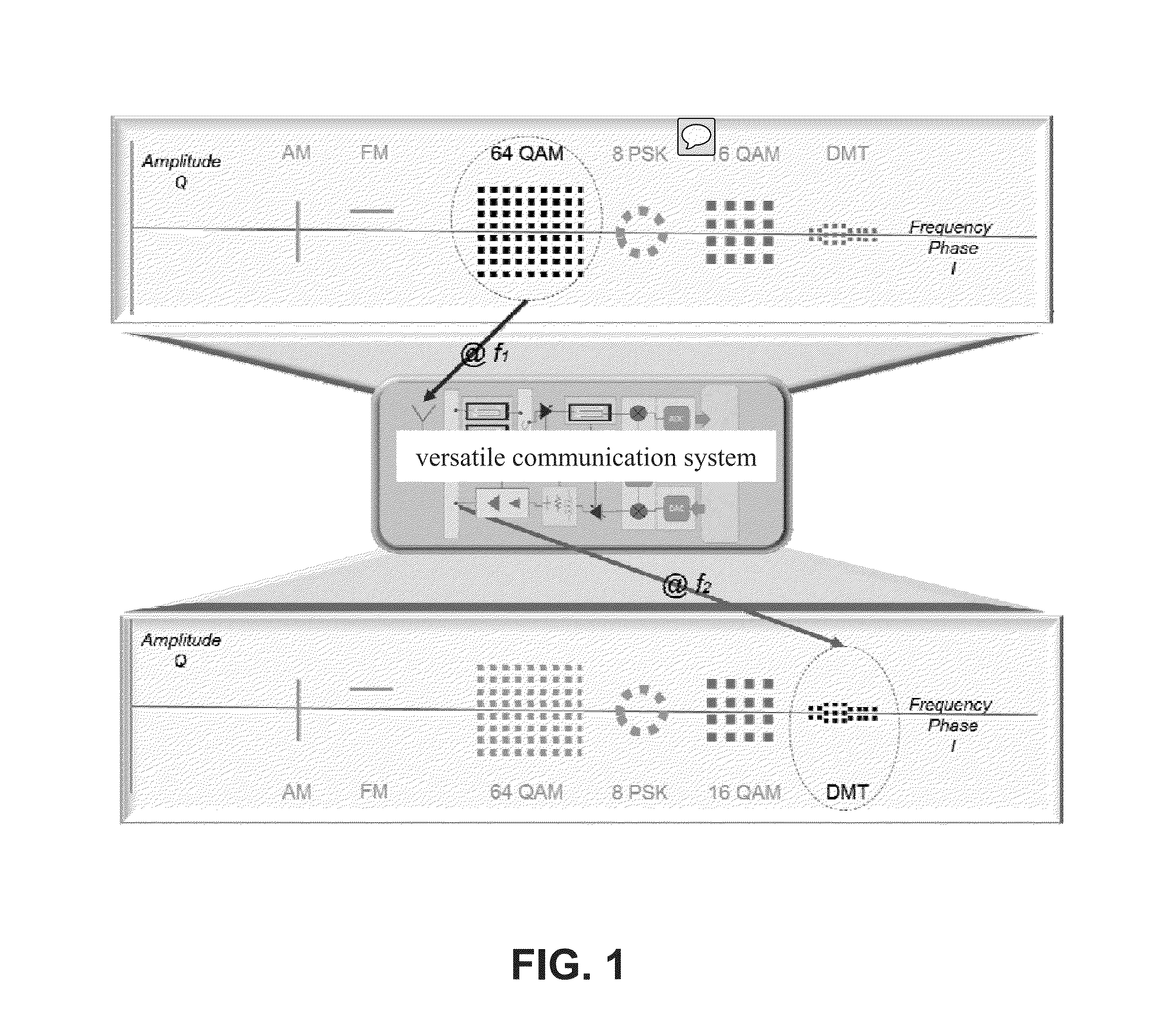
[0018]The software-defined radio (SDR) concept has long been recognized as a desirable system configuration for versatile communication systems and has been driving architectural innovation in recent years. The primary objective is to define / control communication channels by software (see FIG. 1) so that the resulting radio is capable of receiving and generating a variety of waveforms in different frequency bands, different power levels, and different dynamic ranges. FIG. 1 shows a versatile communication system 10 that is capable of receiving any modulated waveform at any frequency. Using software-defined / controlled architecture, this system can also generate any waveforms for transmission at different frequency bands.

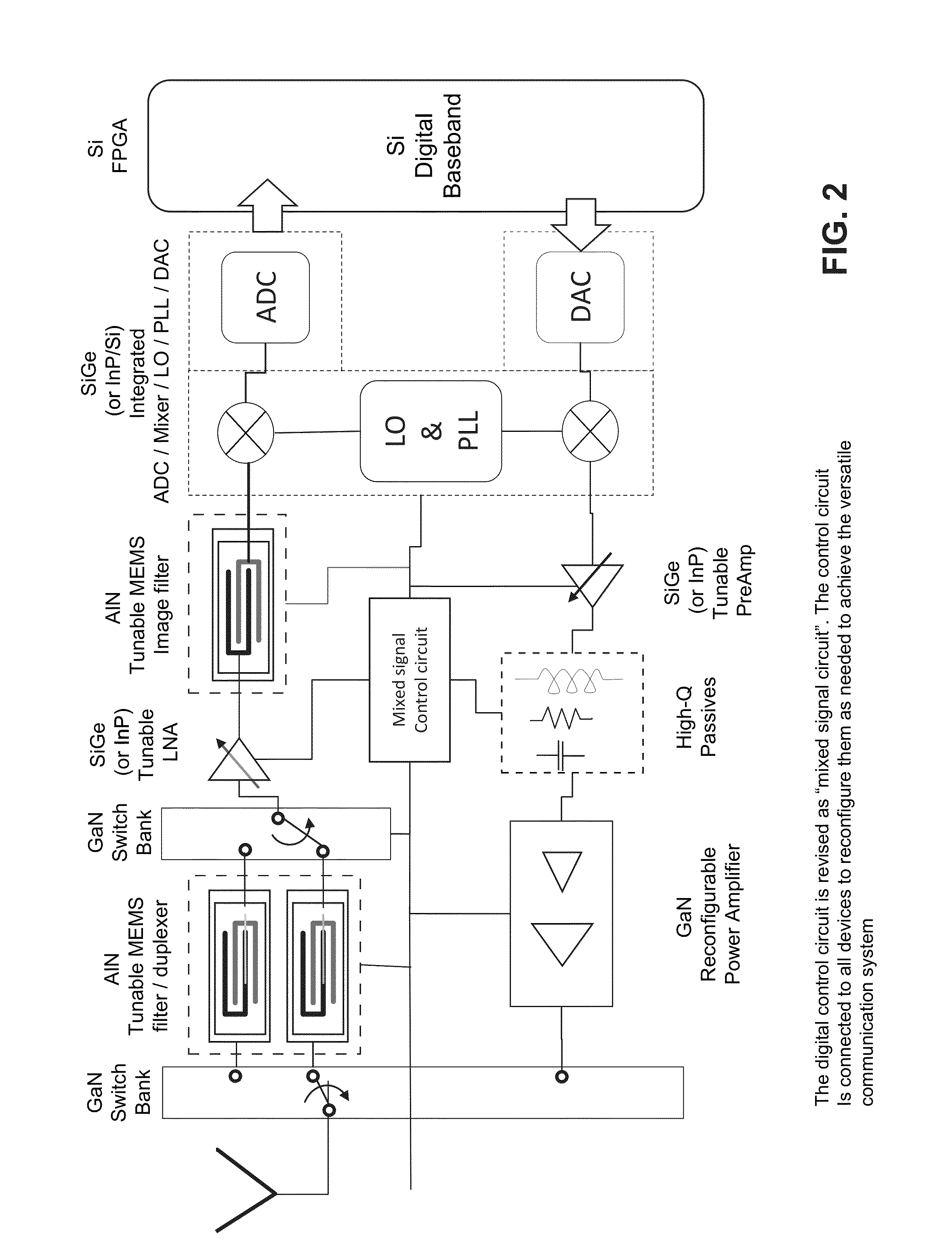
[0019]The present invention also concerns a novel integration m...


PUM


Abstract

A communication system front-end architecture and a method of fabricating same are disclosed in which a diverse set of semiconductor technologies and device types (including CMOS, SiGe CMOS, InP HBTs (heterojunction bipolar transistors), InP HEMTs (high electron mobility transistors), GaN HEMTs, SiC devices, any number from a diverse set of MEMS sensors and actuators, and potentially photonics) is merged onto a single silicon, or other material substrate to thereby enable the development of smaller, lighter, and higher performance systems.

Description

[0001]This application claims the benefit of U.S. Provisional Application No. 61 / 657,320, filed, Jun. 8, 2012, the entire contents of which are incorporated herein by reference.[0002]The present invention is directed to communication systems, and more particularly to a A communication system front-end architecture in which a diverse set of semiconductor technologies and device types (including CMOS, SiGe CMOS, InP HBTs (heterojunction bipolar transistors), InP HEMTs (high electron mobility transistors), GaN HEMTs, SiC devices, any number from a diverse set of MEMS sensors and actuators, and potentially photonics) is merged onto a single silicon, or other material substrate to thereby enable the development of smaller, lighter, and higher performance systems.BACKGROUND OF THE INVENTION[0003]There is increased need and market demand for communication systems that can operate in multiple frequency bands as well as using different modulation techniques. Additionally, the military is ver...

Claims


Application Information

Patent Timeline
Patent Type & Authority Applications(United States)
IPC IPC(8): H04B1/40H01L25/00
CPCH04B1/40H01L25/50H01L24/24H01L2224/24137H01L2924/13064H01L23/5389H03H3/02H03H9/02228H03H9/605H03H9/70H01L2924/1461H01L2924/1305H01L2924/12036H01L2924/13063H01L2224/04105H01L2924/00
Inventor OZGUR, MEHMETPEDERSEN, MICHAELHUFF, MICHAEL A.
Owner FOR NAT RES INITIATIVES
Why Eureka
Try Eureka