

Semiconductor device
a semiconductor and device technology, applied in the field of semiconductor devices, can solve problems such as the degradation of the field-effect mobility of transistors, and achieve the effects of high field-effect mobility, high reliability of semiconductor devices, and the ability to prevent the change of electrical characteristics of transistors including oxide semiconductors
- Summary
- Abstract
- Description
- Claims
- Application Information
AI Technical Summary
Benefits of technology
Problems solved by technology
Method used
Image

Examples
embodiment 1
[0063]In this embodiment, one embodiment of a semiconductor device and a method for manufacturing the semiconductor device are described with reference to FIGS. 2A to 2C and FIGS. 3A to 3E. In this embodiment, a bottom-gate transistor including an oxide semiconductor layer is described as one example of a semiconductor device.
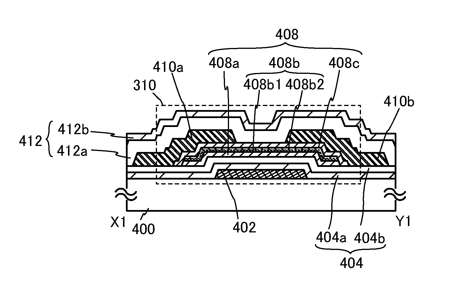
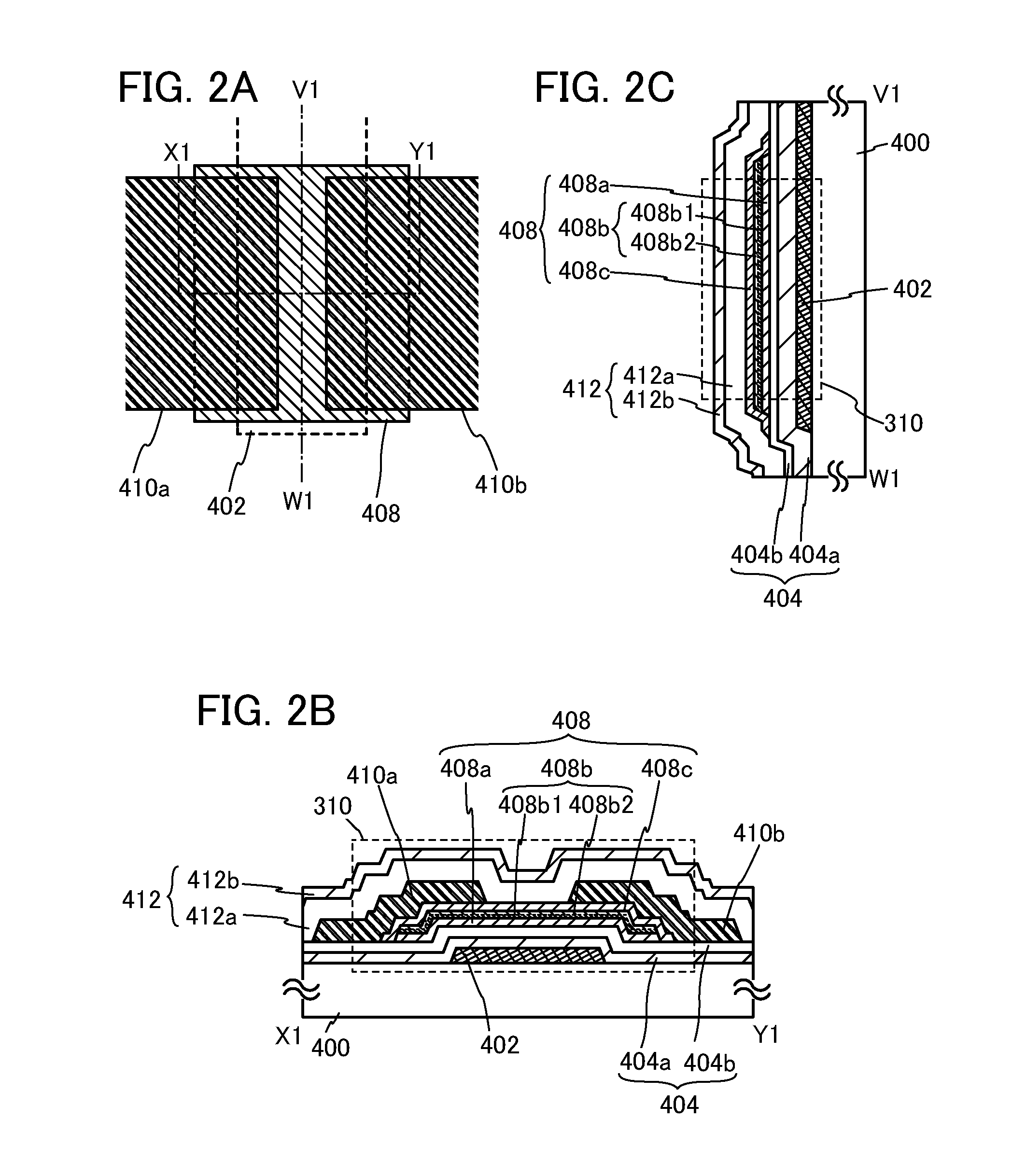
[0064]FIGS. 2A to 2C illustrate a structural example of a transistor 310. FIG. 2A is a plan view of the transistor 310, FIG. 2B is a cross-sectional view taken along X1-Y1 in FIG. 2A, and FIG. 2C is a cross-sectional view taken along V1-W1 in FIG. 2A.
[0065]The transistor 310 illustrated in FIGS. 2A to 2C includes a gate electrode layer 402 which is provided over a substrate 400 having an insulating surface, a gate insulating layer 404 over the gate electrode layer 402, an oxide semiconductor stack 408 which is on and in contact with the gate insulating layer 404 and overlaps with the gate electrode layer 402, and a source electrode layer 410a and a drain electr...
embodiment 2
[0131]In this embodiment, an example of a method for manufacturing a semiconductor device which is different from that described in Embodiment 1 is described with reference to FIGS. 10A to 10E. Embodiment 1 can be applied to the same portions as Embodiment 1 or portions having functions similar to those of Embodiment 1, and therefore, description thereof is not omitted. In addition, detailed description of the same portions is not repeated.
[0132]First, in a manner similar to the process illustrated in FIGS. 3A to 3C, the gate insulating layer 404 including the gate insulating layer 404a and the gate insulating layer 404b is formed over the substrate 400, the island-shaped first oxide semiconductor layer 408a and the island-shaped second oxide semiconductor layer 408b are formed over the gate insulating layer 404, and the oxide semiconductor film 407c is formed to cover the first oxide semiconductor layer 408a and the second oxide semiconductor layer 408b.
[0133]Then, a conductive fi...
embodiment 3
[0146]In this embodiment, a semiconductor device having a different structure from the semiconductor device described in Embodiment 1 or 2 and a method for manufacturing the semiconductor device are described with reference to FIG. 12, FIGS. 16A to 16C, and FIGS. 17A to 17D. In this embodiment, a bottom-gate transistor is described as an example of the semiconductor device. Embodiment 1 or 2 can be applied to the same portions as Embodiment 1 or 2 or portions having functions similar to those of Embodiment 1 or 2; therefore, repetitive description thereof is omitted. In addition, detailed description of the same portions is not repeated.
[0147]FIGS. 16A to 16C illustrate a structural example of a transistor 330. FIG. 16A is a plan view of the transistor 330, FIG. 16B is a cross-sectional view taken along X2-Y2 in FIG. 16A, and FIG. 16C is a cross-sectional view taken along V2-W2 in FIG. 16A.
[0148]The transistor 330 illustrated in FIGS. 16A to 16C is similar to the transistor 310 illu...
PUM
 Abstract
Description
Claims
Application Information