Semiconductor device

a semiconductor and semiconductor technology, applied in semiconductor devices, electric lighting sources, electric light sources, etc., can solve the problems of electrical characteristics that vary among transistors, and achieve the effects of reducing the electrical characteristics of transistors including oxide semiconductor films, and reducing the electrical characteristics of transistors

Active Publication Date: 2014-01-02
SEMICON ENERGY LAB CO LTD
View PDF5 Cites 16 Cited by
  • Summary
  • Abstract
  • Description
  • Claims
  • Application Information

AI Technical Summary

Benefits of technology

[0016]A nitride insulating film which releases hydrogen molecules less than 5×10²¹ molecules/cm3, preferably less than or equal to 3×10²¹ molecules/cm3, more preferably less than or equal to 1×10²¹ molecules/cm3, and ammonia molecules less than 1×10²² molecules/cm3, preferably less than or equal to 5×10²¹ molecules/cm3, more preferably less than or equal to 1×10²¹ molecules/cm3 by heating is provided over a transistor including an oxide semiconductor film, whereby the amount of hydrogen and nitrogen which are moved from the nitride insulating film to the oxide semiconductor film can be reduced. Further, entry of hydrogen contained in water to the oxide semiconductor film from the outside can be suppressed.
[0017]Further, as a gate insulating film of a transistor including an oxide semiconductor film, a nitride ins...

Problems solved by technology

Further, there is a problem in that elec...

Method used


Image

  • Semiconductor device
  • Semiconductor device
  • Semiconductor device

Examples


embodiment 1

[0049]In this embodiment, a semiconductor device of one embodiment of the present invention and a method for manufacturing the semiconductor device is described with reference to drawings.

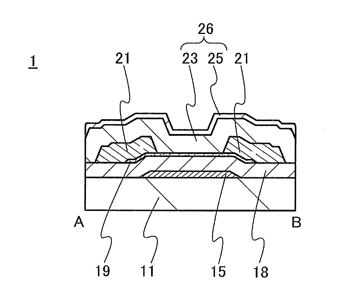
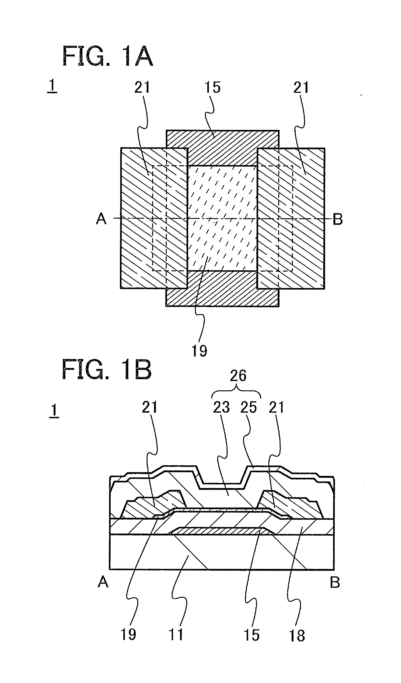
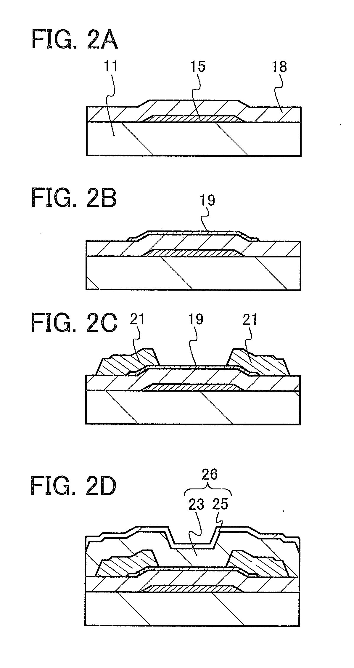
[0050]FIGS. 1A and 1B are a top view and a cross-sectional view of a transistor 1 included in a semiconductor device. FIG 1A is a top view of the transistor 1 and FIG. 1B is a cross-sectional view taken along dashed-dotted line A-B in FIG. 1A. Note that in FIG. 1A, a substrate 11, some components of the transistor 1 (e.g., a gate insulating film 18), an insulating film 23, a nitride insulating film 25, and the like are omitted for simplicity.

[0051]The transistor 1 illustrated in FIGS. 1A and 1B includes a gate electrode 15 provided over the substrate 11, the gate insulating film 18 formed over the substrate 11 and the gate electrode 15, an oxide semiconductor film 19 overlapping with the gate electrode 15 with the gate insulating film 18 provided therebetween, and a pair of electrodes 21 in contact...

embodiment 2

[0162]In this embodiment, a transistor having a structure different from that of Embodiment 1 will be described with reference to FIGS. 3A and 3B. A transistor 3 shown in this embodiment is a top-gate transistor, which is different from the transistors in Embodiment 1.

[0163]FIGS. 3A and 3B are a top view and a cross-sectional view of the transistor 3. FIG. 3A is a top view of the transistor 3, and FIG. 3B is a cross-sectional view taken along dashed-dotted line A-B in FIG. 3A. Note that in FIG. 3A, a substrate 31, a base insulating film 33, some components of the transistor 3 (e.g., an insulating film 37 and a nitride insulating film 39), and the like are omitted for simplicity.

[0164]The transistor 3 illustrated in FIGS. 3A and 3B includes an oxide semiconductor film 34 over the base insulating film 33, a pair of electrodes 35 in contact with the oxide semiconductor film 34, a gate insulating film 40 in contact with the base insulating film 33, the oxide semiconductor film 34, and t...

embodiment 3

[0198]In this embodiment, a transistor having a different structure from the transistors in Embodiment 1 and Embodiment 2 will be described with reference to FIG. 5. A transistor 5 of this embodiment includes a plurality of gate electrodes facing each other with an oxide semiconductor film provided therebetween.

[0199]The transistor 5 illustrated in FIG. 5 includes the gate electrode 15 provided over the substrate 11, the gate insulating film 18 formed over the substrate 11 and the gate electrode 15, the oxide semiconductor film 19 overlapping with the gate electrode 15 with the gate insulating film 18 provided therebetween, and the pair of electrodes 21 in contact with the oxide semiconductor film 19. The protective film 26 including the insulating film 23 and the nitride insulating film 25 is formed over the gate insulating film 18, the oxide semiconductor film 19, and the pair of electrodes 21. Further, a gate electrode 61 overlapping with the oxide semiconductor film 19 with the ...


PUM


Abstract

In a transistor including an oxide semiconductor film, movement of hydrogen and nitrogen to the oxide semiconductor film is suppressed. Further, in a semiconductor device using a transistor including an oxide semiconductor film, a change in electrical characteristics is suppressed and reliability is improved. A transistor including an oxide semiconductor film and a nitride insulating film provided over the transistor are included, and an amount of hydrogen molecules released from the nitride insulating film by thermal desorption spectroscopy is less than 5×10²¹ molecules/cm3, preferably less than or equal to 3×10²¹ molecules/cm3, more preferably less than or equal to 1×10²¹ molecules/cm3, and an amount of ammonia molecules released from the nitride insulating film by thermal desorption spectroscopy is less than 1×10²² molecules/cm3, preferably less than or equal to 5×10²¹ molecules/cm3, more preferably less than or equal to 1×10²¹ molecules/cm3.

Description

TECHNICAL FIELD[0001]The present invention relates to a semiconductor device including a field-effect transistor and a method for manufacturing the semiconductor device.BACKGROUND ART[0002]Transistors used for most flat panel displays typified by a liquid crystal display device and a light-emitting display device are formed using silicon semiconductors such as amorphous silicon, single crystal silicon, and polycrystalline silicon provided over glass substrates. Further, transistors formed using the silicon semiconductors are used in integrated circuits (ICs) and the like.[0003]In recent years, a technique in which, instead of a silicon semiconductor, a metal oxide exhibiting semiconductor characteristics is used for transistors has attracted attention. Note that in this specification, a metal oxide exhibiting semiconductor characteristics is referred to as an oxide semiconductor.[0004]For example, a technique is disclosed in which a transistor is manufactured using zinc oxide or an ...

Claims


Application Information

Patent Timeline
IPC IPC(8): H01L29/24H05B44/00
CPCH01L29/247H01L29/78606H01L29/7869
Inventor SASAKI, TOSHINARIHAMOCHI, TAKASHIMIYAMOTO, TOSHIYUKINOMURA, MASAFUMIKOEZUKA, JUNICHIOKAZAKI, KENICHI
Owner SEMICON ENERGY LAB CO LTD
Why Eureka
Try Eureka