Method of manufacturing single crystal ingot, and single crystal ingot and wafer manufactured thereby

a manufacturing method and technology of single crystal ingots, which are applied in the direction of crystal growth process, polycrystalline material growth, crystal growth process, etc., can solve the problems of poor uniformity, poor rrg characteristics of n-type heavily doped single crystal ingots, and difficult crystal growth through heavy doping. yield and other issues to achieve the effect of improving yield

Inactive Publication Date: 2014-01-16
LG SILTRON
View PDF14 Cites 189 Cited by
  • Summary
  • Abstract
  • Description
  • Claims
  • Application Information

AI Technical Summary

Benefits of technology

[0016]Embodiments provide a method of manufacturing an N-type heavily doped single crystal ingot having an uniformity of the in-plane RES value of a wafer controlled within 3%, and a single crystal ingot and a wafer manufactured thereby.
[0017]Also, according to the embodiments, a high-quality N-type heavily doped single crystal ingot having yield improved by control of a RRG within 5% and a wafer may be grown.
[0018]For example, according to the embodiment, with respect to N-type crystal gro

Problems solved by technology

According to the related art, in an N-type heavily doped single crystal ingot, crystal growth through heavy doping may be particularly difficult because a dopant introduced to adjust resistivity has volatile characteristics having a melting point lower than that of silicon (Si).
Accordingly, resistivity (RES) at the edge becomes higher than that at the center, and thus the N-type heavily doped single crystal ingot may have poor RRG characteristics in comparison to a P-type heavily doped single crystal in

Method used


Image

  • Method of manufacturing single crystal ingot, and single crystal ingot and wafer manufactured thereby
  • Method of manufacturing single crystal ingot, and single crystal ingot and wafer manufactured thereby
  • Method of manufacturing single crystal ingot, and single crystal ingot and wafer manufactured thereby

Examples


embodiment

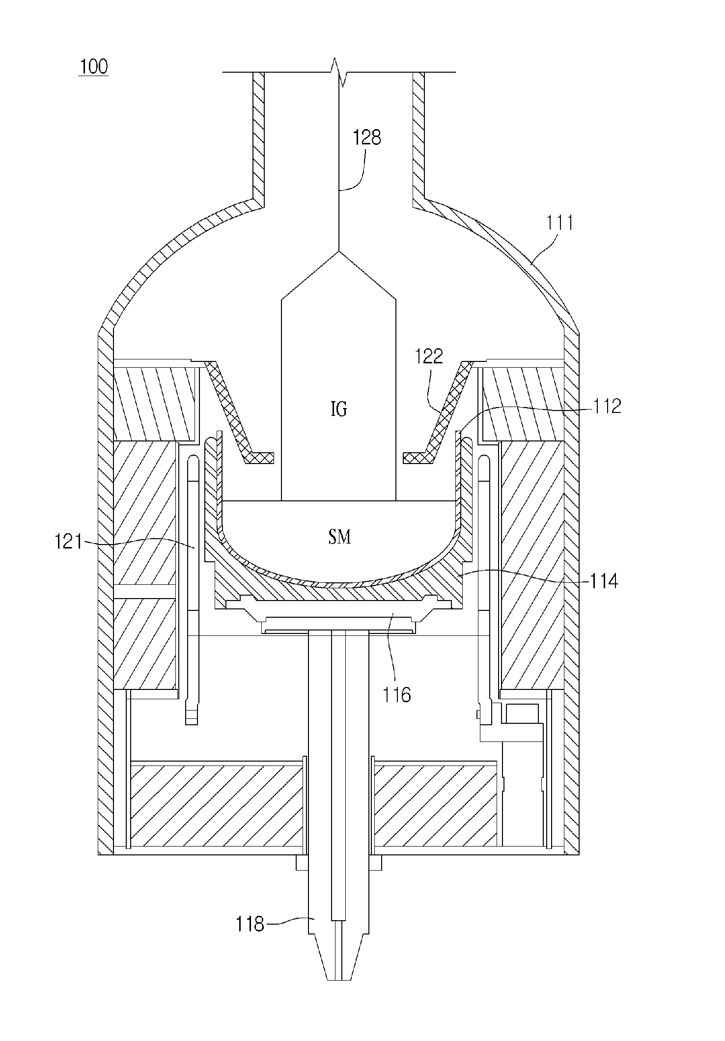
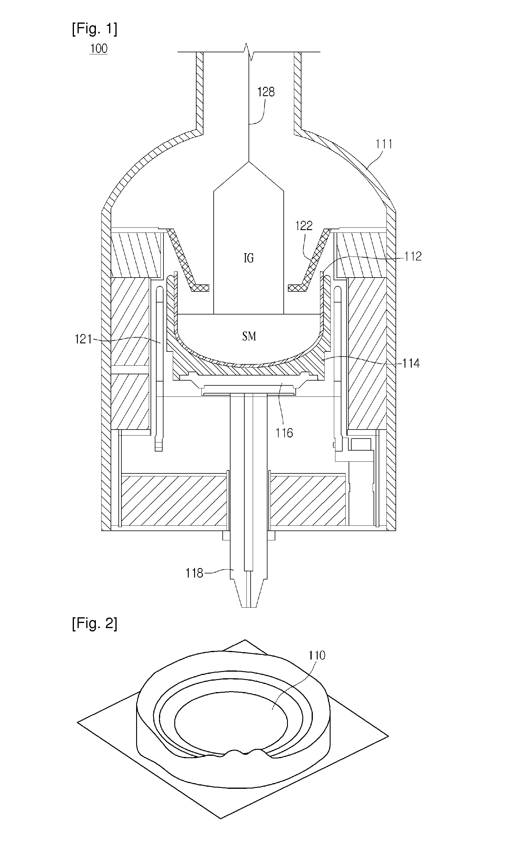
[0027]FIG. 1 is an exemplary view illustrating a single crystal ingot grower used for a method of manufacturing a single crystal ingot according to an embodiment.

[0028]A silicon single crystal ingot grower 100 according to the embodiment may include a chamber 111, a quartz crucible 112, a heater 121, and a pulling means 128.

[0029]For example, the silicon single crystal ingot grower 100 according to the embodiment may include the quartz crucible 112 containing a silicon melt SM and a graphite crucible 114 supporting the quartz crucible 112 by covering a part of an external lower portion thereof, as hot zone structures in the chamber 111, and a supporting structure 116 for supporting a load is disposed under the graphite crucible 114, in which the supporting structure 116 may be combined with a pedestal 118 connected to a rotary driving device (not shown) to be rotated and moved up and down.

[0030]The chamber 111 provides a space, in which predetermined processes for growing a single c...


PUM


Abstract

A method of manufacturing a single crystal ingot, and a single crystal ingot and a wafer manufactured thereby are provided. The method of manufacturing a single crystal ingot according to an embodiment includes forming a silicon melt in a crucible inside a chamber, preparing a seed crystal on the silicon melt, and growing a single crystal ingot from the silicon melt, and pressure of the chamber may be controlled in a range of 90 Torr to 500 Torr.

Description

CROSS-REFERENCE TO RELATED APPLICATIONS[0001]The present application is a national phase application of P.C.T. application PCT / KR2012 / 001992 filed Mar. 20, 2012, which claims the priority benefit of Korean patent application 10-2011-0027632 filed Mar. 28, 2011, the disclosures of which are incorporated herein by reference.BACKGROUND OF THE INVENTION[0002]1. Field of the Invention[0003]The present disclosure relates to a method of manufacturing a single crystal ingot, and a single crystal ingot and a wafer manufactured thereby.[0004]2. Description of the Related Art[0005]A wafer must be manufactured in order to manufacture a semiconductor, and single crystal silicon must first be grown in a form of an ingot in order to manufacture the wafer. For this purpose, a Czochralski (CZ) method may be used.[0006]According to the related art, in an N-type heavily doped single crystal ingot, crystal growth through heavy doping may be particularly difficult because a dopant introduced to adjust r...

Claims


Application Information

Patent Timeline
IPC IPC(8): H01L29/36H01L21/02
CPCH01L29/36H01L21/02002C30B15/20C30B29/06H01L21/02
Inventor KIM, SANG-HEEHWANG, JUNG-HACHOI, YOUNG-KYUSIM, BOK-CHEOL
Owner LG SILTRON
Why Eureka
Try Eureka