Method for forming fine pattern of semiconductor device using double spacer patterning technology

a technology of double spacers and semiconductor devices, applied in the direction of semiconductor devices, basic electric elements, electrical equipment, etc., can solve the problems of difficult to apply the euv process at a production level, and the difficulty of forming a line/space pattern of 38 nm or less through a conventional exposure method, and achieve uniform line width

Inactive Publication Date: 2014-01-16
SK HYNIX INC
View PDF7 Cites 21 Cited by
  • Summary
  • Abstract
  • Description
  • Claims
  • Application Information

AI Technical Summary

Benefits of technology

[0010]One or more exemplary embodiments are directed to a method of forming a fine pattern of a semiconductor device using a double SPT process. A method according to an embodiment of the present invention is capable of implementing a line / space pattern having a fine and uniform line width.

Problems solved by technology

With reduction in a design rule of a semiconductor device, it is difficult to form a line / space pattern of 38 nm or less through a conventional exposure method using ArF immersion exposure equipment that employs a numerical aperture (NA) of 1.35 or less.
However, it is difficult to apply the EUV process at a production level due to various limitations in exposure source power, mechanism, reticle, lack of resist, and the like.

Method used


Image

  • Method for forming fine pattern of semiconductor device using double spacer patterning technology
  • Method for forming fine pattern of semiconductor device using double spacer patterning technology
  • Method for forming fine pattern of semiconductor device using double spacer patterning technology

Examples


Embodiment Construction

.”

BRIEF DESCRIPTION OF THE DRAWINGS

[0046]The above and other aspects, features and other advantages of the subject matter of the present disclosure will be more clearly understood from the following detailed description taken in conjunction with the accompanying drawings.

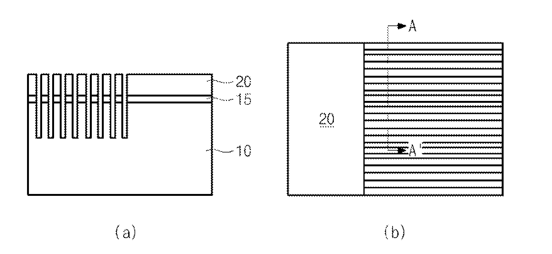
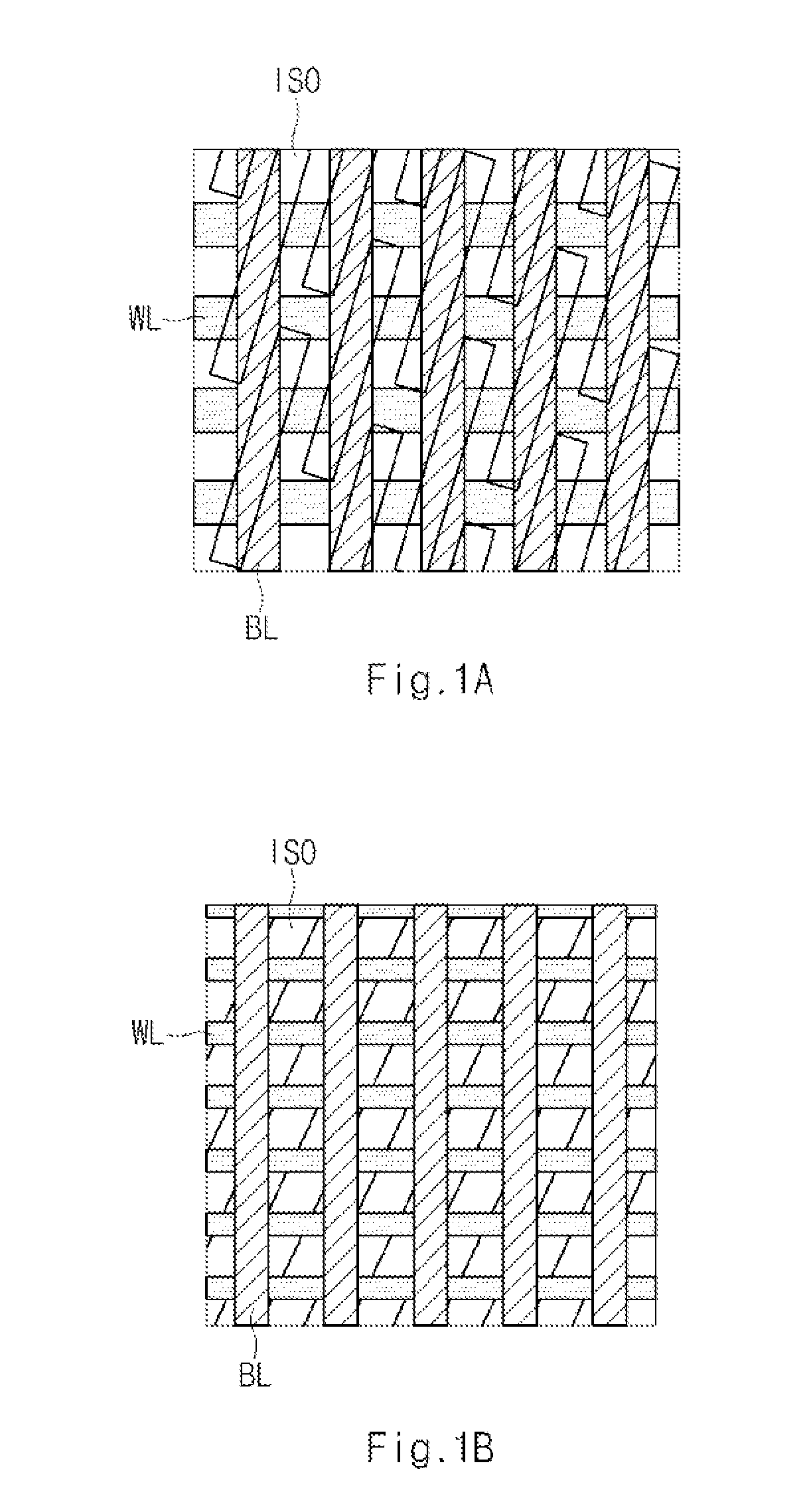
[0047]FIGS. 1A and 1B are views illustrating isolation structures according to exemplary embodiments of the present invention.

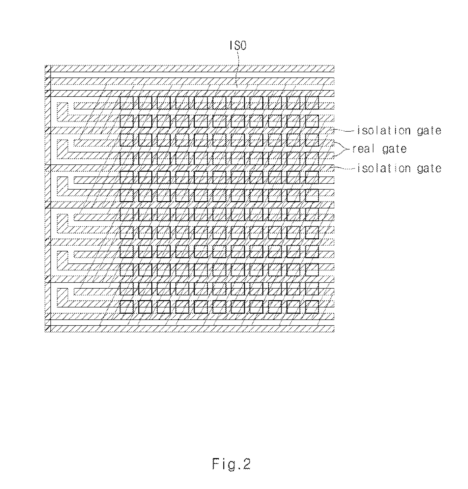
[0048]FIG. 2 is a view illustrating a gate in the isolation structure illustrated in FIG. 1A.

[0049]FIGS. 3A to 3D are schematics views illustrating positive spacer patterning technology (SPT) and negative SPT.

[0050]FIGS. 4A to 4L are views illustrating a method of forming a fine pattern of a semiconductor device according to a first exemplary embodiment of the present invention.

[0051]FIGS. 5A to 5O are views illustrating a method of forming a fine pattern of a semiconductor device according to a second exemplary embodiment of the present invention.

DETAILED DESCRIPTION

[0052]Hereinafter, exempl...


PUM

PropertyMeasurementUnit
wavelengthaaaaaaaaaa
work functionaaaaaaaaaa

Abstract

A method of forming a fine pattern of a semiconductor device using double SPT process, which is capable of implementing a line and space pattern having a uniform fine line width by applying a double SPT process including a negative SPT process, is provided. The method includes a first SPT process and a second SPT process and the second SPT process includes a Negative SPT process.

Description

CROSS-REFERENCES TO RELATED APPLICATION[0001]This application claims priority under 35 U.S.C. 119(a) to Korean application number 10-2012-0076220, filed on Jul. 12, 2012, in the Korean Patent Office, which is incorporated by reference in its entirety.BACKGROUND OF THE INVENTION[0002]1. Technical Field[0003]The present invention relates to a method of forming a fine pattern of a semiconductor device, and more particularly, to a method of forming a fine pattern of a semiconductor device using double spacer patterning technology.[0004]2. Related Art[0005]With reduction in a design rule of a semiconductor device, it is difficult to form a line / space pattern of 38 nm or less through a conventional exposure method using ArF immersion exposure equipment that employs a numerical aperture (NA) of 1.35 or less. An exposure source (extreme ultraviolet (EUV) having a wavelength of 13.4 nm) has been used to develop a pattern of 30 nm or less. However, it is difficult to apply the EUV process at ...

Claims


Application Information

Patent Timeline
Patent Type & Authority Applications(United States)
IPC IPC(8): H01L21/48
CPCH01L21/4846H01L2924/0002H01L21/28132H01L21/3086H10B41/42H01L21/0273
Inventor LEE, KI LYOUNGBOK, CHEOL KYUKIM, WON KYU
Owner SK HYNIX INC
Why Eureka
Try Eureka