Nitride-based semiconductor device and method of manufacturing nitride-based semiconductor device

Inactive Publication Date: 2014-01-23
SAMSUNG ELECTRONICS CO LTD
View PDF5 Cites 1 Cited by
  • Summary
  • Abstract
  • Description
  • Claims
  • Application Information

AI Technical Summary

Benefits of technology

The patent text describes a method for making a nitride-based semiconductor device that improves the surface quality of an aluminum gallium nitride layer and reduces leakage current.

Problems solved by technology

However, a structure of an AlGaN / GaN HFET with a high electron mobility may have a disadvantage in that leakage current flowing along a surface may decrease a device property, due to an unstable AlGaN surface.

Method used


Image

  • Nitride-based semiconductor device and method of manufacturing nitride-based semiconductor device
  • Nitride-based semiconductor device and method of manufacturing nitride-based semiconductor device
  • Nitride-based semiconductor device and method of manufacturing nitride-based semiconductor device

Examples


Embodiment Construction

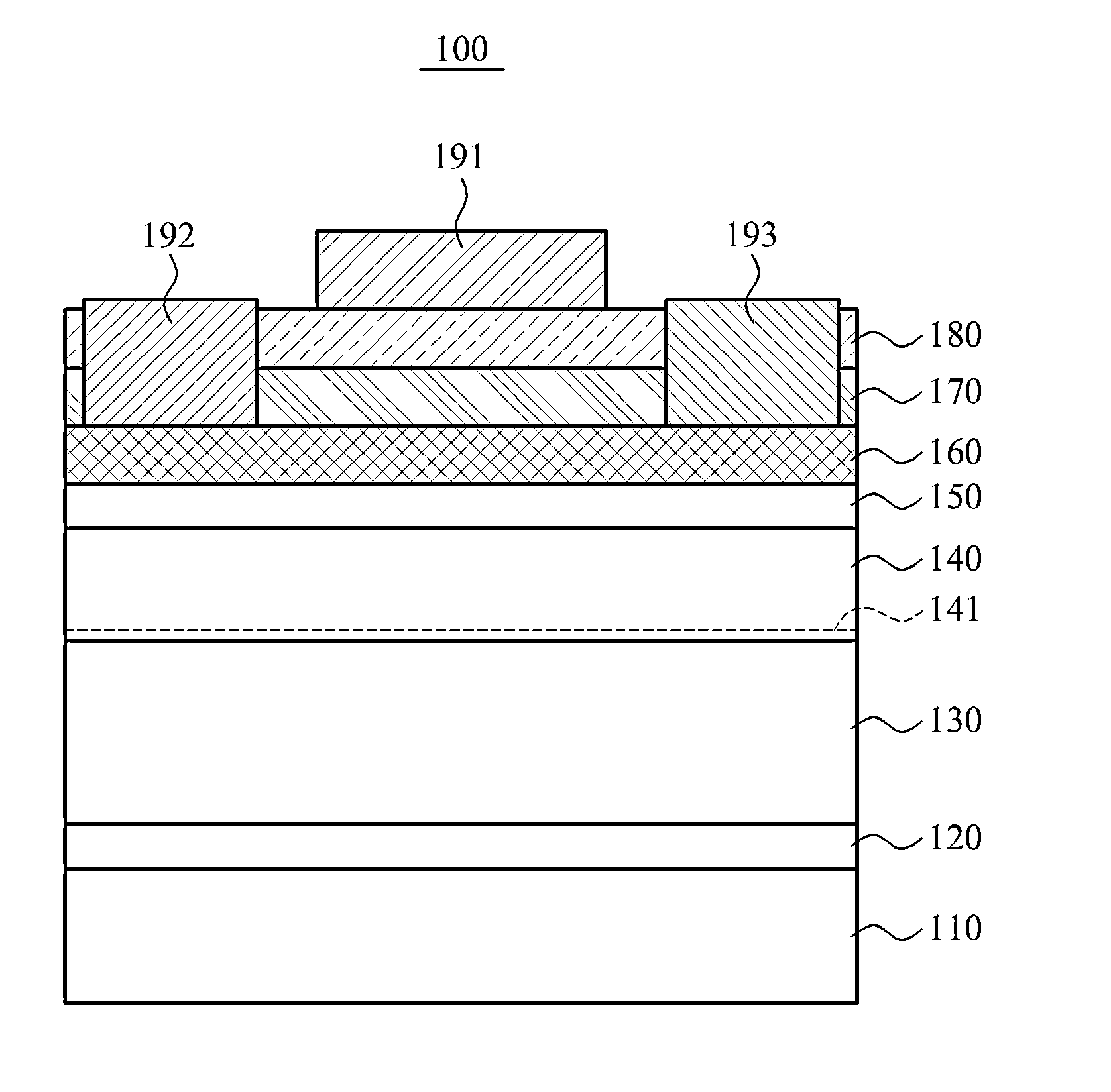
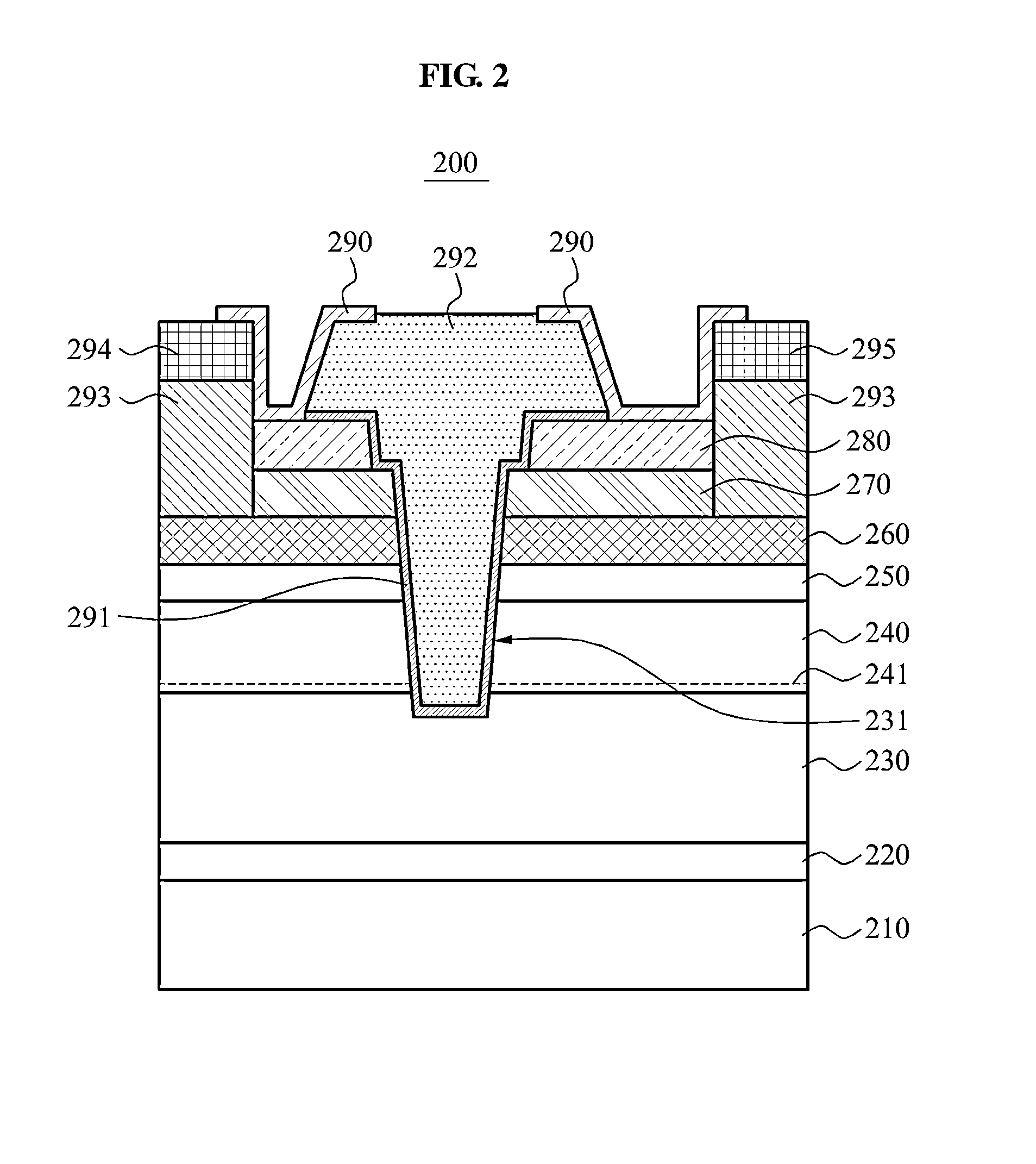
[0041]Reference will now be made in detail to exemplary embodiments of the present inventive concept, examples of which are illustrated in the accompanying drawings, wherein like reference numerals may refer to like elements throughout. Exemplary embodiments are described below to explain the present inventive concept by referring to the figures.

[0042]Throughout the specification, when it describes that each of a layer, a side, a chip, and the like is formed “on” or “under” a layer, a side, a chip, and the like, the term “on” may include “directly on” and “indirectly on by interposing another element therebetween,” and the term “under” may include “directly under” and “indirectly under by interposing another element therebetween.” A non-limiting example for “on” or “under” of each element may be determined based on a corresponding drawing.

[0043]The size of each element in the drawings may be exaggerated for ease of description, and may not indicate the actual size of the element.

[00...


PUM


Abstract

In a nitride-based semiconductor device, an undoped gallium nitride (GaN) layer is formed on an aluminum gallium nitride (AlGaN) layer, and a silicon carbon nitride (SixC1-xN) functional layer is formed on the undoped GaN layer.

Description

CROSS-REFERENCE TO RELATED APPLICATION[0001]This application claims the benefit of Korean Patent Application No. 10-2012-0079360, filed on Jul. 20, 2012, in the Korean Intellectual Property Office, the disclosure of which is incorporated herein by reference in its entirety.BACKGROUND[0002]1. Field of the Present Inventive Concept[0003]The present inventive concept relates to a nitride-based semiconductor device and a method of manufacturing the nitride-based semiconductor device, and more particularly, to a nitride-based semiconductor device and a method of manufacturing the nitride-based semiconductor device that improves surface roughness of an aluminum gallium nitride (AlGaN) layer and that reduces leakage current.[0004]2. Description of the Related Art[0005]As information communication technologies have been considerably developed globally, communication technologies for high-speed and large-capacity signal communication have been rapidly developed. In particular, due to an incr...

Claims


Application Information

Patent Timeline
IPC IPC(8): H01L29/267
CPCH01L29/267H01L21/0237H01L21/02447H01L21/02458H01L21/02505H01L21/02521H01L21/02529H01L29/0657H01L29/2003H01L29/26H01L29/42316H01L29/66462H01L29/7787H01L29/737
Inventor LEE, JAE HOON
Owner SAMSUNG ELECTRONICS CO LTD
Why Eureka
Try Eureka