Systems and methods for laser splitting and device layer transfer

a technology which is applied in the field of laser splitting and device layer transfer, can solve the problems of inhomogeneity formed in the uniform matrix of solid materials, affecting the quality of semiconductor devices, so as to reduce disadvantages or eliminate disadvantages

Active Publication Date: 2014-02-06
BEAMREACH SOLAR INC
View PDF1 Cites 163 Cited by
  • Summary
  • Abstract
  • Description
  • Claims
  • Application Information

AI Technical Summary

Benefits of technology

[0018]Therefore, a need has arisen for device layer fabrication from a donor wafer. In accordance with the disclosed subject matter, laser processing methods for fabricating a device layer which substantially eliminates or reduces disadvantages associated with previously developed device layer fabrication methods and systems.

Problems solved by technology

The laser beam penetrates internally up (or down) to a depth from the solid surface and is then absorbed at a small site with dense energy concentration, resulting in some inhomogeneity formed in uniform matrix of the solid material.
Such inhomogeneity in the uniform matrix of mono-crystalline wafers often introduces a large amount of stress localized at the selected sites, resulting in breakage of Si—Si bonds in the proximate vicinity of the selected site which leads to micro-cracks.
Formation of cavities, voids, and pores may also take place under extreme conditions of abnormal light absorption due to increased light absorption coefficient during heating.

Method used


Image

  • Systems and methods for laser splitting and device layer transfer
  • Systems and methods for laser splitting and device layer transfer
  • Systems and methods for laser splitting and device layer transfer

Examples


Embodiment Construction

[0052]The following description is not to be taken in a limiting sense, but is made for the purpose of describing the general principles of the present disclosure. The scope of the present disclosure should be determined with reference to the claims. Exemplary embodiments of the present disclosure are illustrated in the drawings, like numbers being used to refer to like and corresponding parts of the various drawings.

[0053]And although the present disclosure is described with reference to specific embodiments, such as back-contact solar cells using monocrystalline silicon substrates and other described fabrication materials, one skilled in the art could apply the principles discussed herein to front contact cells, other fabrication materials including alternative semiconductor materials (such as gallium arsenide, germanium, gallium nitride, etc.), technical areas, and / or embodiments without undue experimentation.

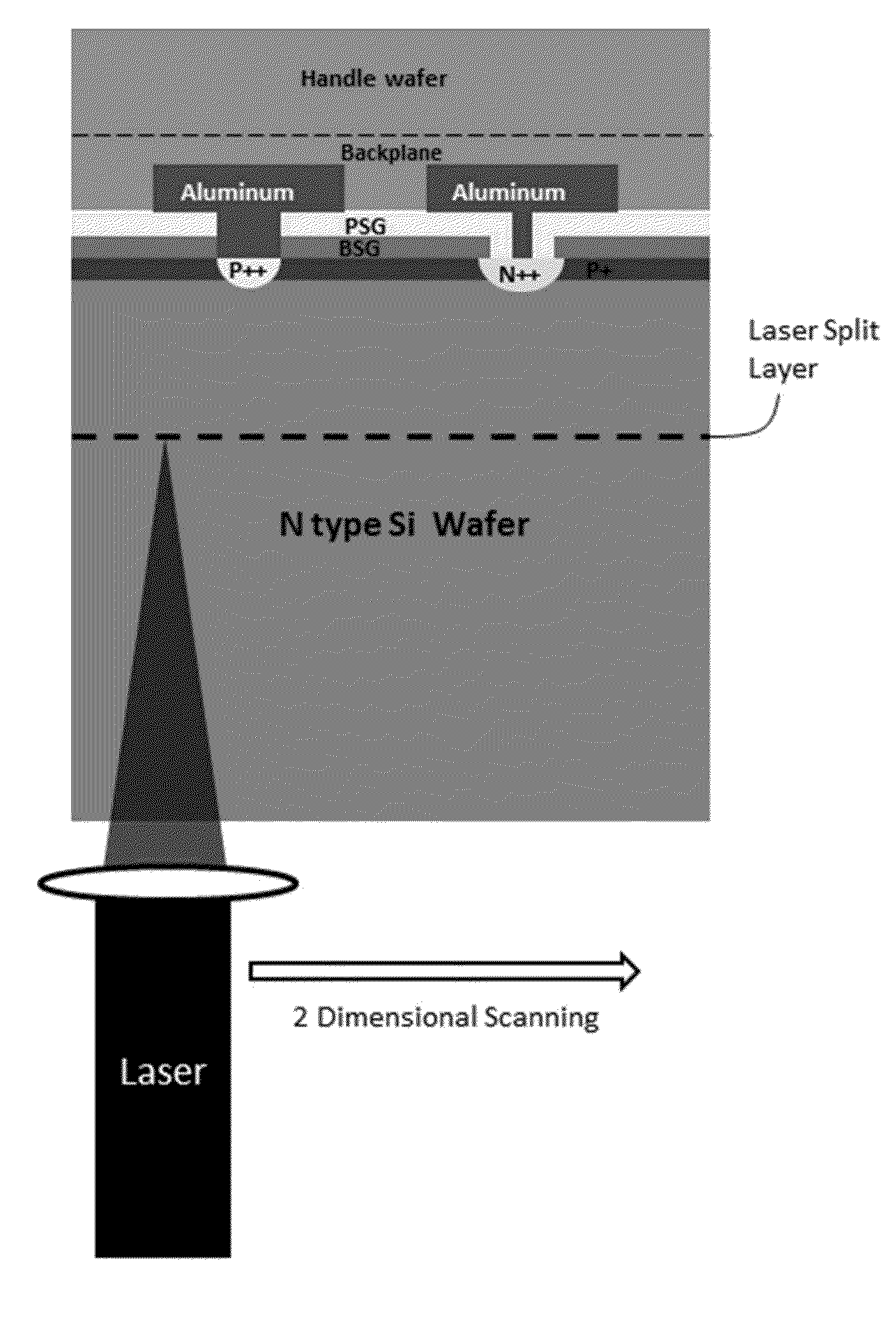
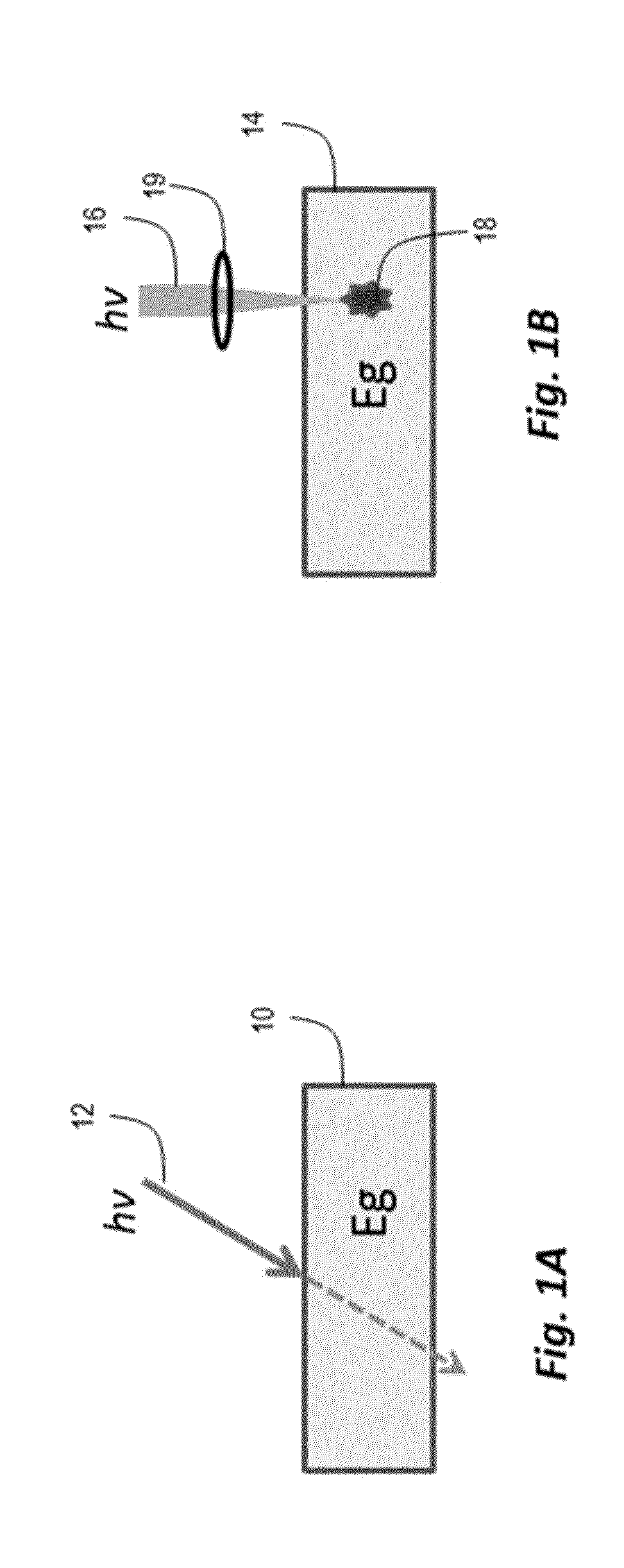
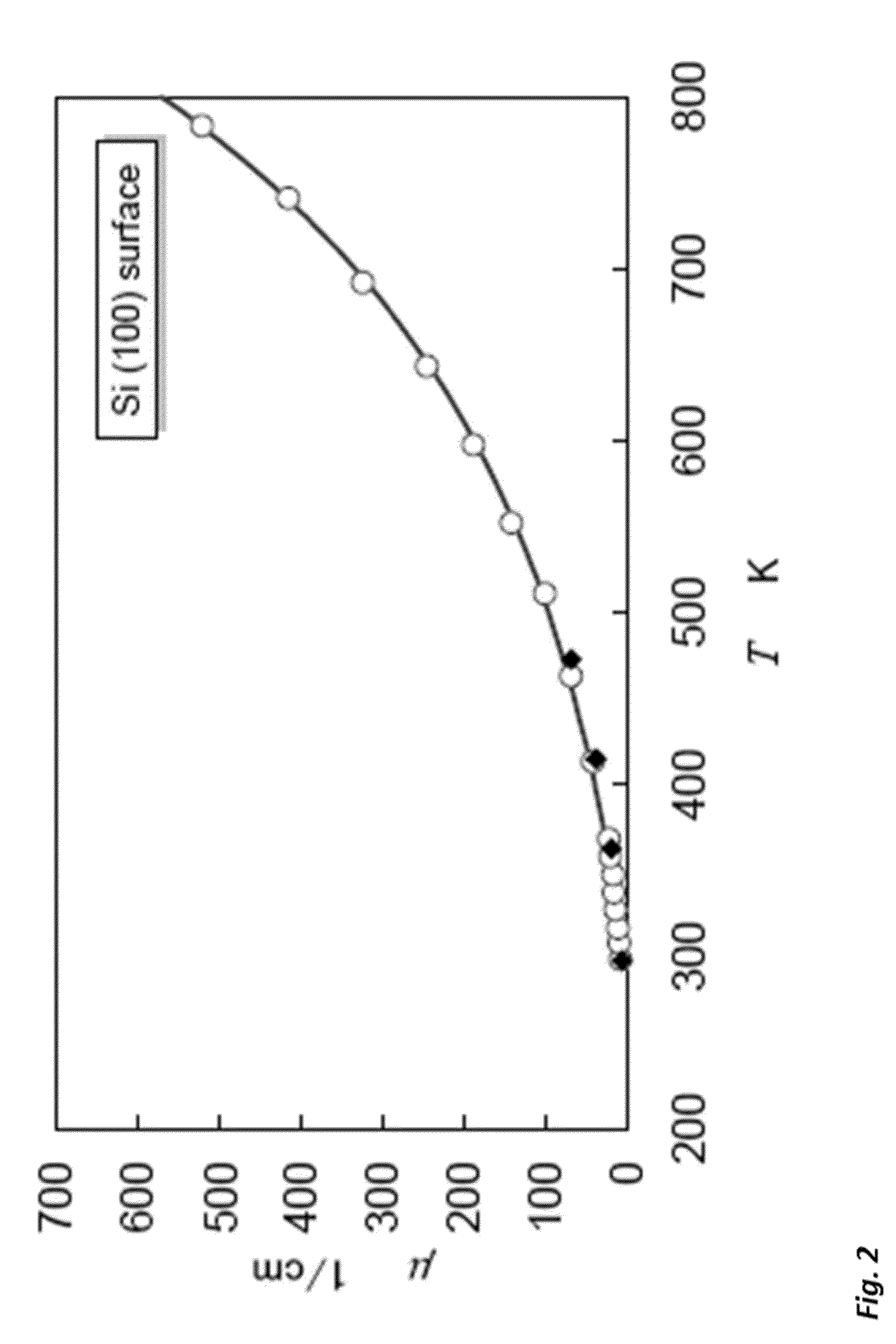
[0054]The embodiments disclosed herein are applicable to splitting or r...


PUM

PropertyMeasurementUnit
absorption coefficientaaaaaaaaaa
sizeaaaaaaaaaa
sizeaaaaaaaaaa

Abstract

Methods and systems are provided for the split and separation of a layer of desired thickness of crystalline semiconductor material containing optical, photovoltaic, electronic, micro-electro-mechanical system (MEMS), or optoelectronic devices, from a thicker donor wafer using laser irradiation.

Description

CROSS-REFERENCE TO RELATED APPLICATIONS[0001]This application claims the benefit of U.S. Provisional Patent App. Nos. 61 / 603,370 filed on Feb. 26, 2012, 61 / 603,894 filed on Feb. 27, 2012, 61 / 609,347 filed on Mar. 11, 2012, and 61 / 708,477 filed on Oct. 1, 2012 which are hereby incorporated by reference in their entirety.FIELD OF THE INVENTION[0002]The present disclosure relates in general to the fields of semiconductor devices, and more particularly to laser processing of semiconductor device layers.BACKGROUND[0003]FIG. 1A is a cross-sectional diagram of energy particles 12 (for example photons from a laser beam) passing through semiconductor substrate 10 showing normal absorption of photons. In FIG. 1A, incident photons carry the optical energy without causing any mass transport. The material layer absorbs the energetic particles, in which the absorption passes are classified into two categories: Linear and Nonlinear absorption. Normal absorption of photons in semiconductor material...

Claims


Application Information

Patent Timeline
Patent Type & Authority Applications(United States)
IPC IPC(8): H01L21/304
CPCH01L21/3043H01L21/268H01L21/76254H01L21/304H01L31/1892H01L33/0095B23K26/0093B23K26/0869H01L25/0657H01L2224/32245H01L2224/48091H01L2224/48145H01L2224/48247H01L2224/49107H01L2224/73265H01L2924/1461H01L2924/13091H01L31/022441H01L31/0682B23K26/0006B23K26/702B23K26/082B23K26/0622B81C2201/0192B81C1/0038B81C2201/0194H01L2224/32145Y02E10/547B23K26/50B23K26/53B23K2101/40B23K2103/52H01L2924/00014H01L2924/00H01L2924/00012B23K26/062B23K26/361H01L21/67092H01L21/76259H01L21/78H01L33/0093B42D25/00B23K26/244B81C1/0088H01L21/7813
Inventor YONEHARA, TAKAORANA, VIRENDA V.SEUTTER, SEANMOSLEHI, MEHRDAD M.TAMILMANI, SUBRAMANIAN
Owner BEAMREACH SOLAR INC
Why Eureka
Try Eureka