

Package carrier and manufacturing method thereof
- Summary
- Abstract
- Description
- Claims
- Application Information
AI Technical Summary
Benefits of technology
Problems solved by technology
Method used
Image

Examples
Embodiment Construction
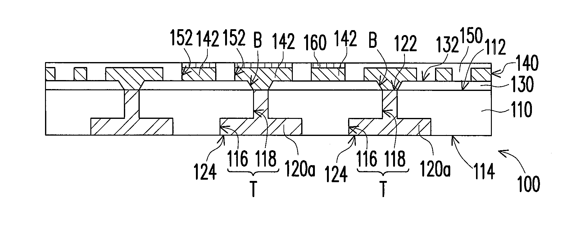
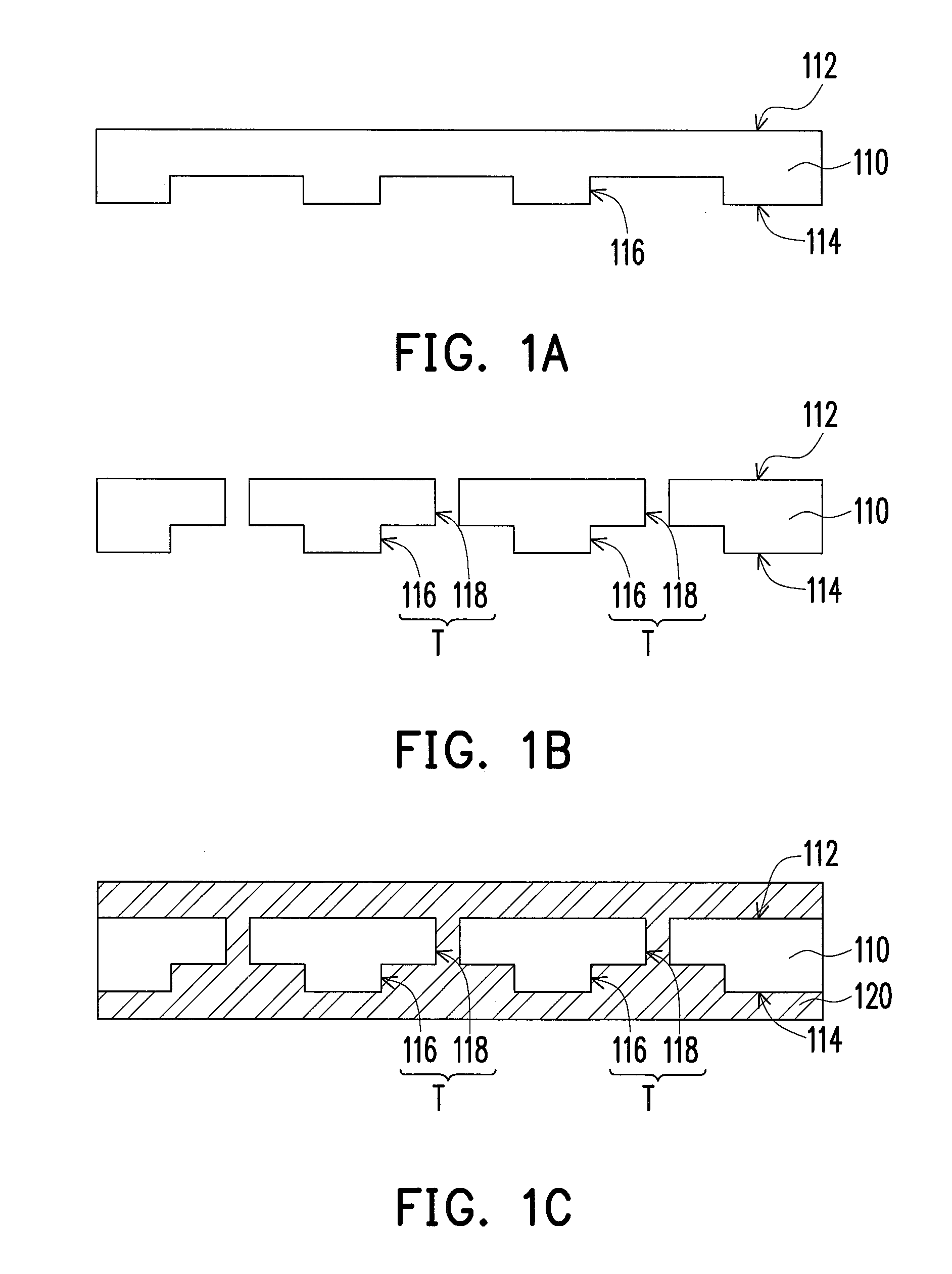
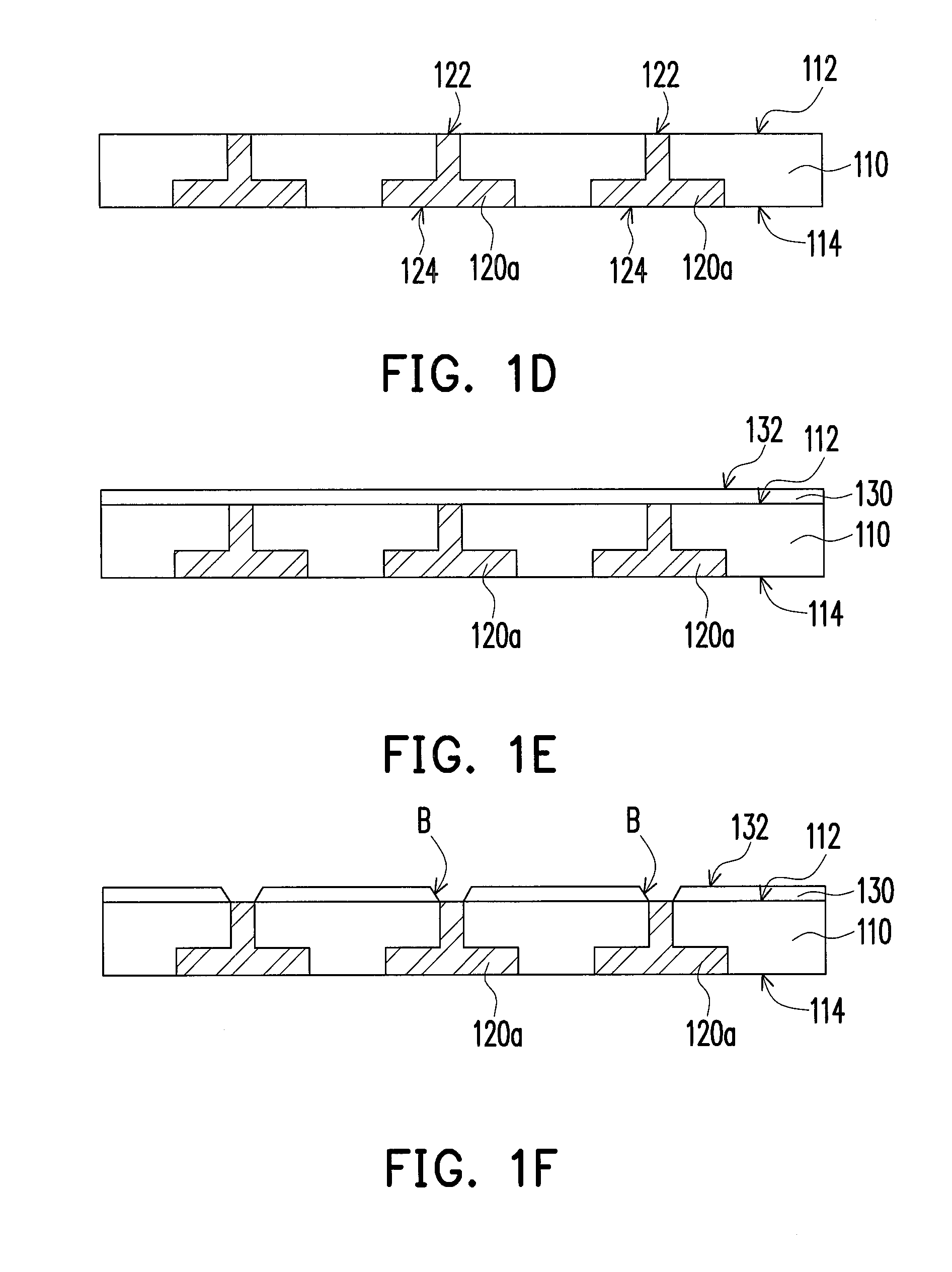
[0030]FIGS. 1A to 1H are schematic cross-sectional views of a manufacturing method of a package carrier according to an embodiment of the invention. According to the manufacturing method of the package carrier of the present embodiment, referring to FIG. 1A, an insulation substrate 110 is provided first. The insulation substrate 110 has an upper surface 112, a lower surface 114 opposite to the upper surface 112 and a plurality of cavities 116, wherein the cavities 116 are located at the lower surface 114 of the insulation substrate 110. Herein, a method of forming the cavities 116 of the insulation substrate 110 is, for example, laser drilling or injection molding. In addition, a material of the insulation substrate 110 is, for example, ABF resin, polymeric materials, silicon fillers or epoxy resin.
[0031]Then, referring to FIG. 1B, through holes 118 passing through the insulation substrate 110 and respectively communicating with the cavities 116 are formed on the upper surface 112 o...
PUM
| Property | Measurement | Unit |
|---|---|---|
| Electrical conductor | aaaaa | aaaaa |
Abstract
Description
Claims
Application Information