

Light emitting device, method of manufacturing the same, and electronic apparatus
- Summary
- Abstract
- Description
- Claims
- Application Information
AI Technical Summary
Benefits of technology
Problems solved by technology
Method used
Image

Examples
first embodiment
Light Emitting Apparatus
[0058]First, an organic electroluminescence (EL) device as a light emitting device of the present embodiment will be described with reference to FIGS. 1 to 3. FIG. 1 is an equivalent circuit view illustrating an electrical configuration of an organic EL device of a first embodiment, FIG. 2 is a schematic plan view illustrating the organic EL device of the first embodiment, and FIG. 3 is a schematic plan view illustrating displacement of a light emitting pixel according to the first embodiment.
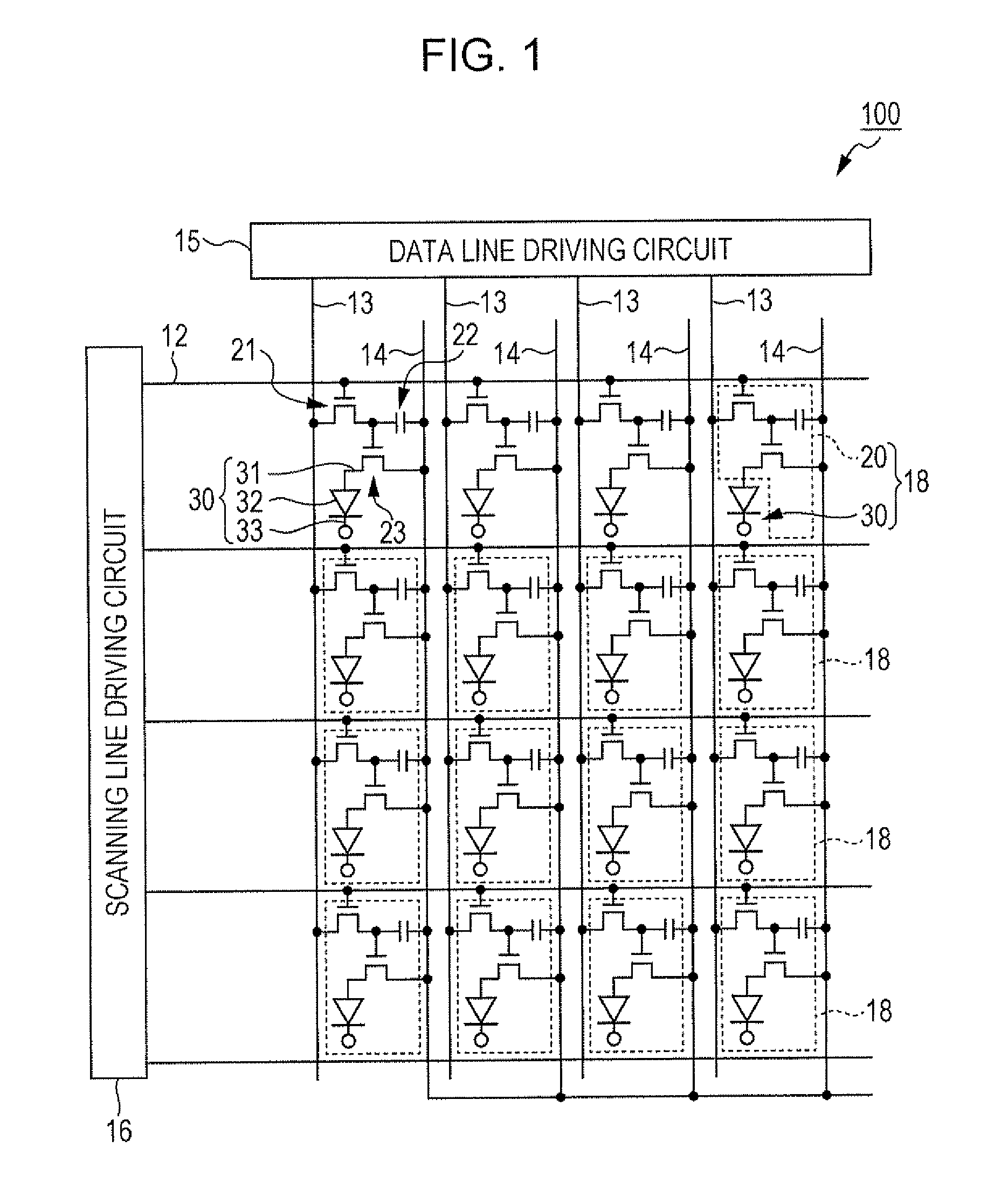
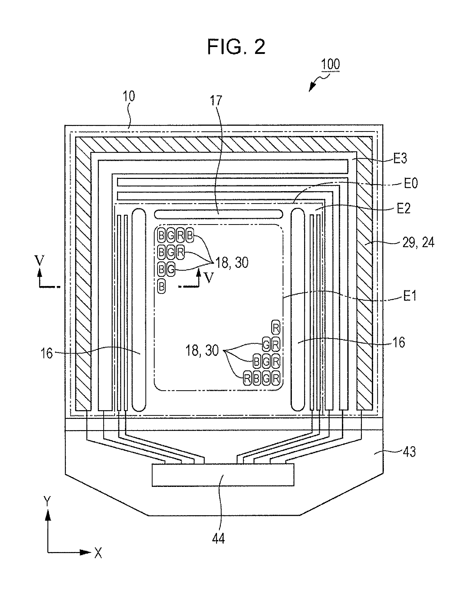
[0059]As illustrated in FIG. 1, an organic EL device 100 as a light emitting device of the embodiment has a plurality of scanning lines 12 and a plurality of data lines 13 which mutually intersect each other and a plurality of power supply lines 14 that are parallel respectively with respect to the plurality of data lines 13 respectively. The organic EL device has a scanning line driving circuit 16 to which the plurality of scanning lines 12 are connected and a data line...
second embodiment
Light Emitting Apparatus
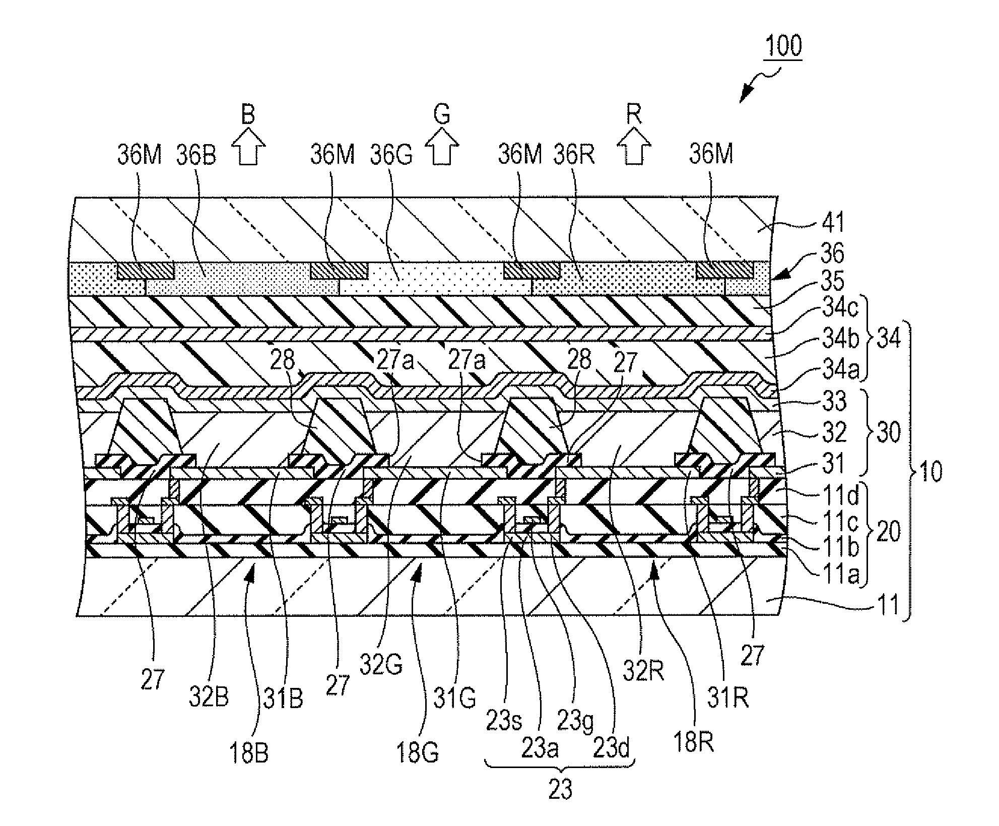
[0113]Next, an organic EL device as a light emitting device of a second embodiment will be described with reference to FIGS. 8 and 9. FIG. 8 is a schematic sectional view illustrating a structure of the organic EL device of the second embodiment, and FIGS. 9A and 9B are schematic sectional views illustrating the structure of the non-display region of the organic EL device of the second embodiment. In addition, the organic EL device as the light emitting device of the second embodiment has a different configuration from the element substrate 10 with respect to the organic EL device 100 of the first embodiment. FIG. 8 corresponds to a sectional view taken along the line VIII-VIII of FIG. 3, and FIGS. 9A and 9B correspond to a sectional view taken along the lines IXA-IXA and IXB-IXB of FIG. 2. Therefore, the same reference numerals will be given to the same configurations as the first embodiment and detailed descriptions will be omitted. Moreover, in FIGS. 8 and...
third embodiment
Electronic Device
[0142]Next, an electronic apparatus of the present embodiment will be described with reference to FIGS. 13 and 14. FIG. 13 is a schematic view illustrating a television as electronic apparatus, and FIG. 14 is a perspective view illustrating a head-mounting display as electronic apparatus.
[0143]As illustrated in FIG. 13, a television (TV) 500 as electronic apparatus of the embodiment is configured to use the organic EL device 100 of the above-described embodiment for the display unit 501. Therefore, since the high reliability can be obtained in the emission lifetime and the width of the non-display region E3 is narrow, as long as a screen size is the same, the TV 500 which is more compact compared to a television of the related art can be provided. Moreover, compared with a case where a liquid crystal display device is employed to the display unit 501, since an illuminating device is not necessary, the thinner TV 500 can be realized.
[0144]As illustrated in FIG. 14, t...
PUM
 Abstract
Description
Claims
Application Information