Semiconductor package and method of fabricating the same

a technology of semiconductors and semiconductor components, applied in the direction of semiconductor devices, semiconductor/solid-state device details, electrical equipment, etc., can solve the problems of reducing the surface area of the chip for storing solder balls, affecting the stability of the chip, so as to prevent the warpage of the package

Inactive Publication Date: 2014-02-13
SILICONWARE PRECISION IND CO LTD
View PDF7 Cites 19 Cited by
  • Summary
  • Abstract
  • Description
  • Claims
  • Application Information

AI Technical Summary

Benefits of technology

[0019]Therefore, the present invention provides a support layer made of silicon or glass for supporting the soft layer so as to prevent warpage of the package. Further, by electrically connecting the first and second RDL structures through the first and second conductive through hole vias, the present invention allows disposing of other packages or electronic elements.

Problems solved by technology

However, the application of the RDL technique or formation of conductive traces on the chip is limited by the size of the chip or the area of the active surface of the chip.
Particularly, along with increased integration and continuous reduction in size, chips lack sufficient surface area for accommodating more solder balls for electrical connection to an external device.
Further, a positional deviation can easily occur to the chip 102 due to softening or expansion of the adhesive film 104 caused by heat, especially during a molding process, thereby adversely affecting the electrical connection between the RDL structure and the electrode pads 108 of the chip 102.
Furthermore, no conductive through hole via is formed in the package and therefore the upper and lower RDL structures cannot be electrically connected to each other.
As such, other packages or electronic elements cannot be disposed on the package.

Method used


Image

  • Semiconductor package and method of fabricating the same
  • Semiconductor package and method of fabricating the same
  • Semiconductor package and method of fabricating the same

Examples


Embodiment Construction

[0024]The following illustrative embodiments are provided to illustrate the disclosure of the present invention, these and other advantages and effects can be apparent to those in the art after reading this specification.

[0025]It should be noted that all the drawings are not intended to limit the present invention. Various modification and variations can be made without departing from the spirit of the present invention. Further, terms, such as “first”, “second”, “on” etc., are merely for illustrative purpose and should not be construed to limit the scope of the present invention.

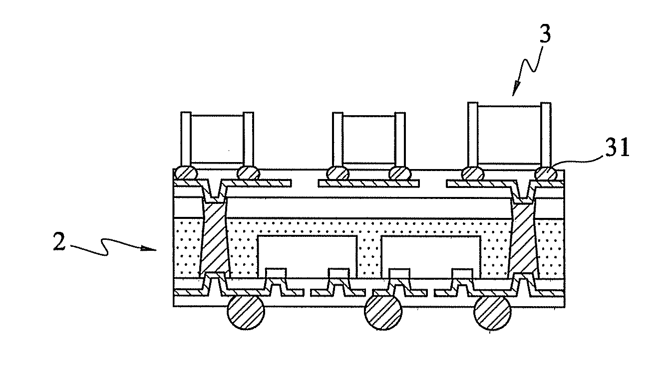
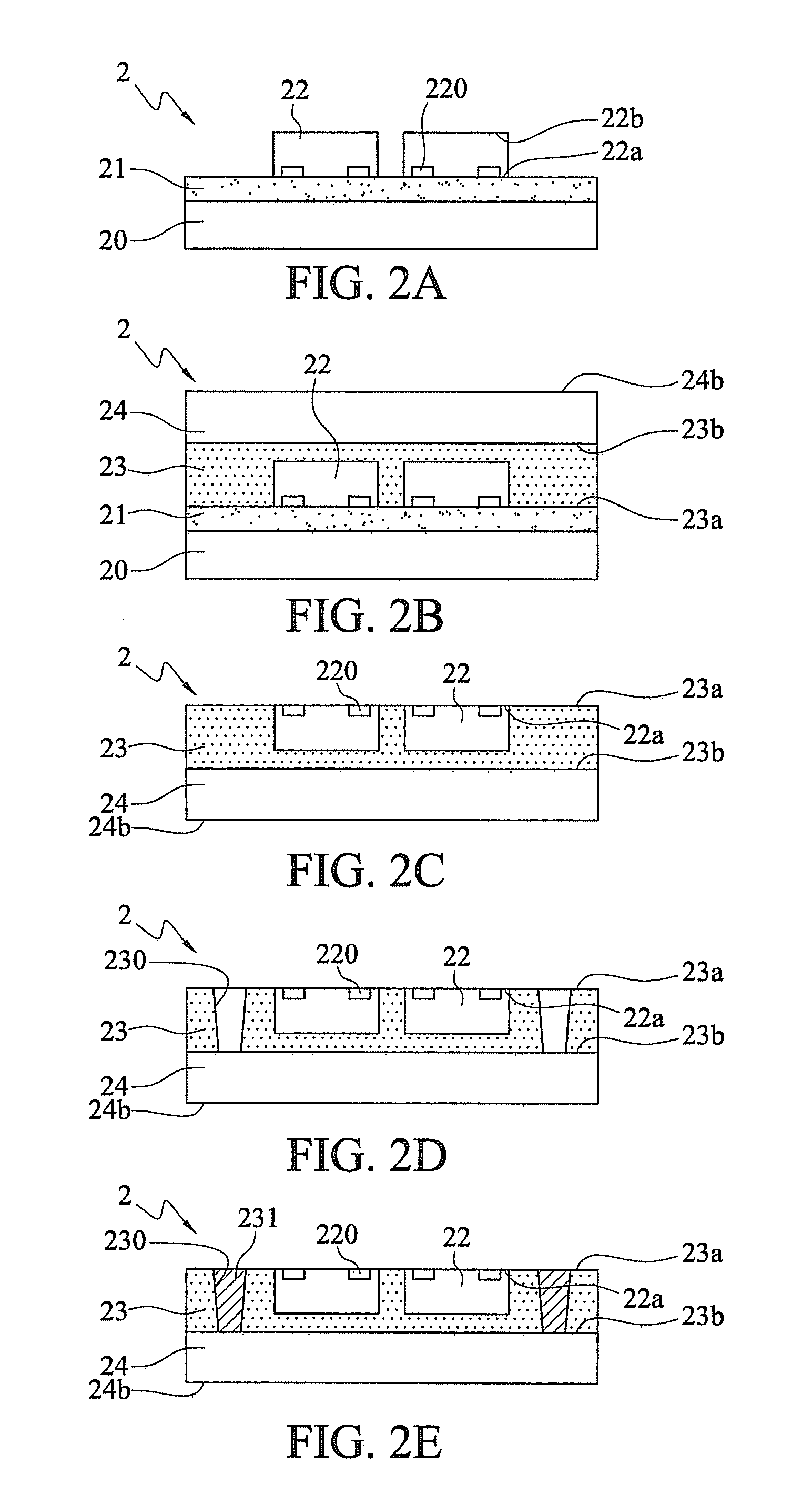
[0026]FIGS. 2A to 2J are cross-sectional views showing a method of fabricating a semiconductor package according to an embodiment of the present invention.

[0027]Referring to FIG. 2A, a carrier 20 is provided with an adhesive layer 21 formed thereon. At least a chip 22 having an active surface 22a with a plurality of electrode pads 220 and a non-active surface 22b opposite to the active surface 22a is provid...


PUM


Abstract

A semiconductor package is provided, which includes: a soft layer having opposite first and second surfaces and first conductive through hole vias; a chip embedded in the soft layer and having an active surface exposed from the first surface of the soft layer; a support layer formed on the second surface of the soft layer and having second conductive through hole vias in electrical connection with the first conductive through hole vias; a first RDL structure formed on the first surface of the soft layer and electrically connected to the active surface of the chip; and a second RDL structure formed on the support layer and electrically connected to the first RDL structure through the first and second conductive through hole vias. The invention prevents package warpage by providing the support layer, and allows disposing of other packages or electronic elements by electrically connecting the RDL structures through the conductive through hole vias.

Description

BACKGROUND OF THE INVENTION[0001]1. Field of the Invention[0002]The present invention relates to semiconductor packages and methods of fabricating the same, and, more particularly, to a wafer level semiconductor package and a method of fabricating the same.[0003]2. Description of Related Art[0004]Along with the development of semiconductor technologies, various package types have been developed for semiconductor products. A chip scale package (CSP) is characterized in that the package size is equal to or slightly greater than a chip disposed in the package.[0005]In a conventional CSP structure as disclosed by U.S. Pat. Nos. 5,892,179, 6,103,552, 6,287,893, 6,350,668 and 6,433,427, a build-up structure is directly disposed on a chip and a redistribution layer (RDL) technique is used to re-route electrode pads of the chip.[0006]However, the application of the RDL technique or formation of conductive traces on the chip is limited by the size of the chip or the area of the active surfac...

Claims


Application Information

Patent Timeline
Patent Type & Authority Applications(United States)
IPC IPC(8): H01L23/48H01L21/60
CPCH01L21/561H01L23/3128H01L25/105H01L2224/32145H01L2224/32225H01L2224/48227H01L2224/73265H01L2225/0651H01L2225/1058H01L2225/06568H01L2225/1035H01L2924/15311H01L23/5389H01L23/49816H01L23/49822H01L23/49827H01L25/0655H01L24/20H01L24/82H01L2224/13022H01L2224/73209H01L2224/12105H01L2224/13024H01L2924/00014H01L24/73H01L2225/1041H01L2924/00012H01L2924/00H01L2224/13099
Inventor LIU, HUNG-WENHSU, HSI-CHANGCHOU, HSIN-HUNGLIAO, HSIN-YICHANG, CHIANG-CHENG
Owner SILICONWARE PRECISION IND CO LTD
Why Eureka
Try Eureka