Nitride semiconductor light emitting device

a technology of light-emitting devices and semiconductors, which is applied in the direction of semiconductor devices, basic electric elements, electrical equipment, etc., can solve the problems of reducing the internal quantum efficiency of the light-emitting layer, and achieve the effect of reducing color non-uniformity

Inactive Publication Date: 2014-02-20
PANASONIC CORP
View PDF0 Cites 15 Cited by
  • Summary
  • Abstract
  • Description
  • Claims
  • Application Information

AI Technical Summary

Benefits of technology

[0019]According to the above aspect, the light distribution characteristic can be controlled more appropriately, or the color non-uniformity can be decreased.

Problems solved by technology

This causes a problem that the internal quantum efficiency of the light emitting layer is decreased due to the quantum-confined Stark effect of the carriers.

Method used


Image

  • Nitride semiconductor light emitting device
  • Nitride semiconductor light emitting device
  • Nitride semiconductor light emitting device

Examples


embodiment 1

[0146]Hereinafter, a semiconductor light-emitting device according to Embodiment 1 of the present disclosure will be described with reference to FIGS. 3A and 3B.

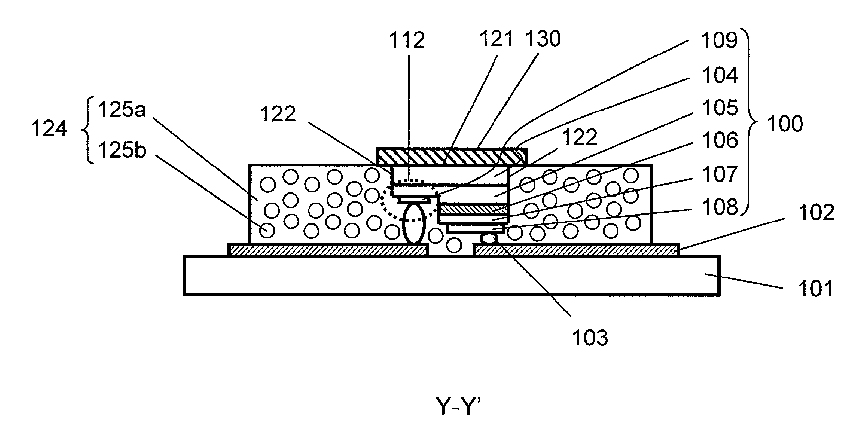
[0147]As shown in FIGS. 3A and 3B, a semiconductor light-emitting device in this embodiment includes a mounting substrate 101, a nitride semiconductor light-emitting chip 100 mounted on the mounting substrate 101, a first light-transmissive member 124 located to the side of the nitride semiconductor light-emitting chip 100, and a second light-transmissive member 126 located in an area above the nitride semiconductor light-emitting chip 100 (“above” refers to a direction opposite to the direction from the nitride semiconductor light-emitting chip 100 toward the mounting substrate 101).

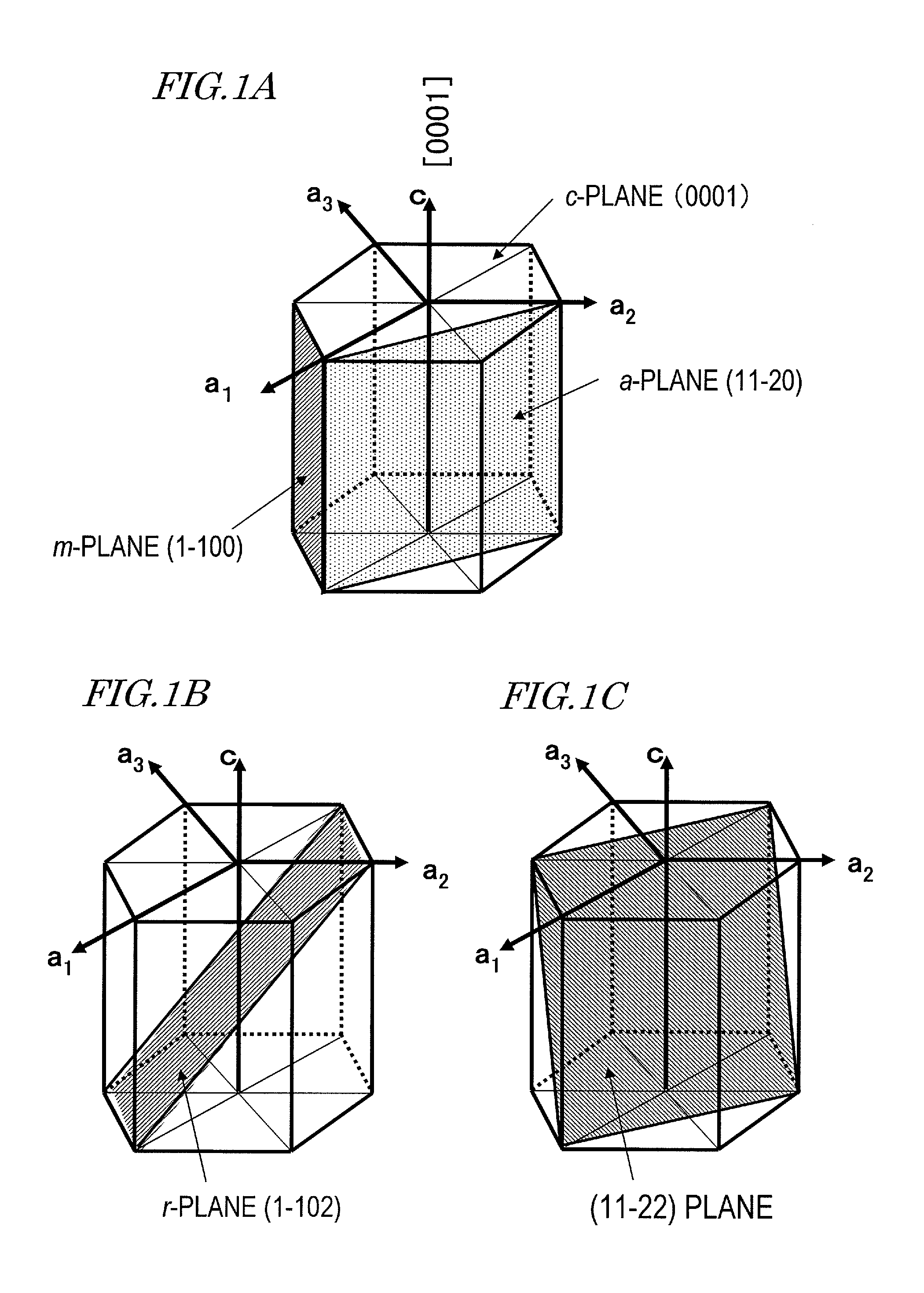
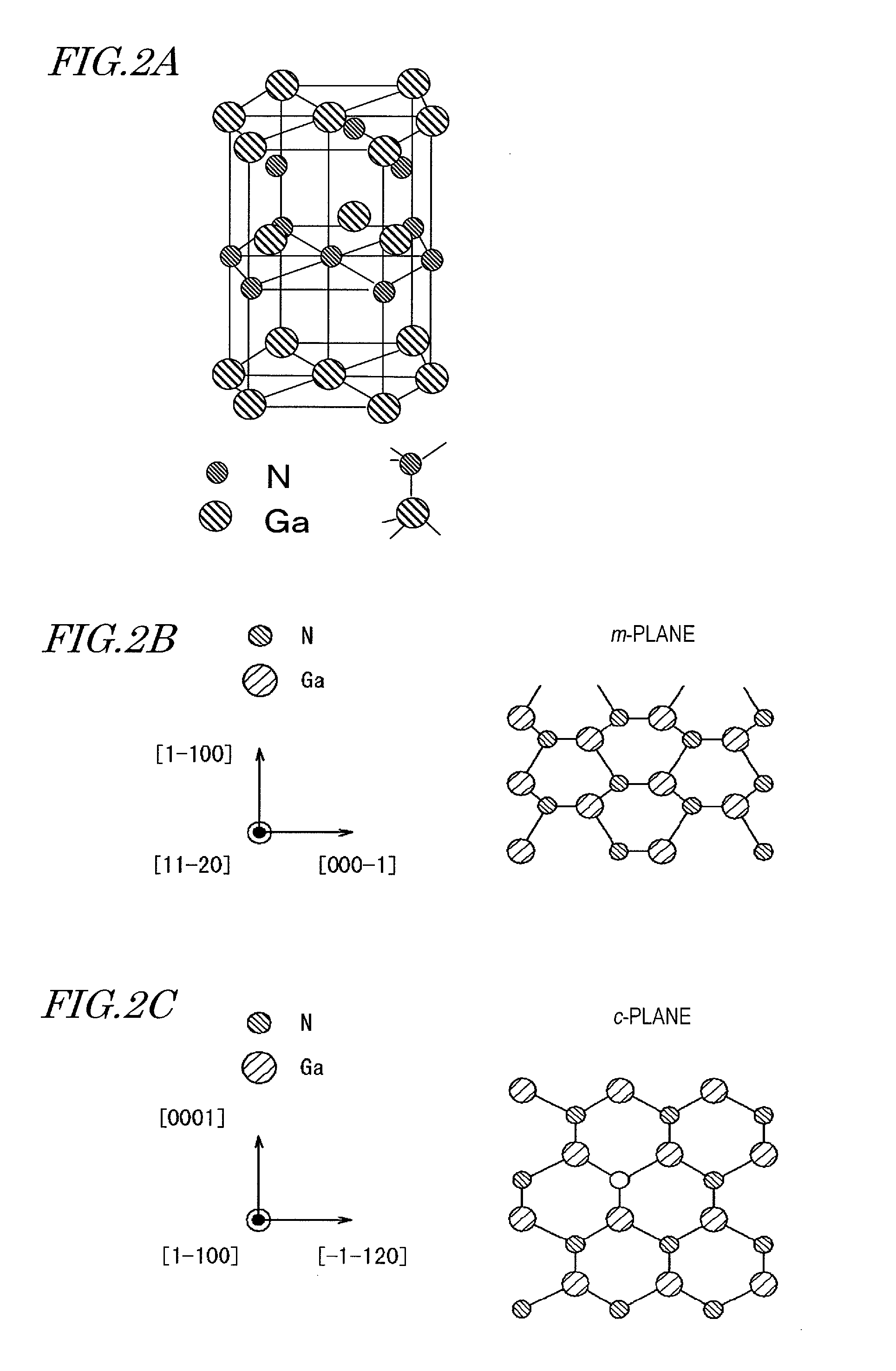
[0148]As shown in FIG. 3B, the nitride semiconductor light-emitting chip 100 includes a substrate 104 including a GaN layer having the m-plane as a main plane (and also a growth plane) (hereinafter, referred to as an “m-plane GaN layer”), an n-t...

embodiment 2

[0201]Hereinafter, a semiconductor light-emitting device according to Embodiment 2 according to the present disclosure will be described with reference to FIGS. 14A through 14F. In FIG. 14, identical elements to those in FIG. 3 will bear identical reference signs thereto and descriptions thereof will be omitted. This will be also applied to the following embodiments. Herein, differences of Embodiment 2 from Embodiment 1 will be described.

[0202]As shown in FIGS. 14A and 148, in Embodiment 2, unlike in Embodiment 1, the first light extraction plane 121 has a plurality of projection and recess portions 104a having a plurality of projection and recess or texture. In the example of FIG. 14B, each projection portion of the projection and recess portions 104a has a generally semi-spherical cross-section in a direction perpendicular to the substrate surface. The projection and recess portions 104a at the rear surface of the substrate 104 can be produced by thinning the substrate 104, formin...

embodiment 3

[0210]Hereinafter, Embodiment 3 according to the present disclosure will be described with reference to FIGS. 15A and 15B.

[0211]FIGS. 15A and 15B are respectively a plan view and a cross-sectional view of a semiconductor light-emitting device in this embodiment. The semiconductor light-emitting device in this embodiment includes a semiconductor light-emitting chip 100, a wavelength converting member 112, and a first light-transmissive member 124. The semiconductor light-emitting device may further include a second light-transmissive member 126. As shown in FIG. 15B, the semiconductor light-emitting chip 100 has a semiconductor stacking structure formed of nitride semiconductors. The semiconductor stacking structure includes a substrate 104 having a GaN layer having the m-plane as a main plane (and also a growth plane) (hereinafter, such a GaN layer will be referred to as an m-plane GaN layer) on at least a surface thereof, an n-type nitride semiconductor layer 105 formed on the main...


PUM


Abstract

A nitride semiconductor light-emitting device includes a nitride semiconductor light-emitting chip including an active layer for outputting polarized light, the active layer having a non-polar plane or a semi-polar plane as a growth plane; and a light-transmissive cover for transmitting light from the active layer. The light-transmissive cover includes a first light-transmissive member located in an area, among areas to the side of the nitride semiconductor light-emitting chip, and in a direction perpendicular to a polarization direction of the polarized light, and a second light-transmissive member located in an area above the nitride semiconductor light-emitting chip. The first light-transmissive member has a higher diffuse transmittance than the second light-transmissive member.

Description

[0001]This is a continuation of International Application No. PCT / JP2013 / 000204, with an international filing date of Jan. 17, 2013, which claims priority of Japanese Patent Applications No. 2012-010950, filed on Jan. 23, 2012, No. 2012-012247, filed on Jan. 24, 2012 and No. 2012-030166, filed on Feb. 15, 2012, the contents of which are hereby incorporated by reference.BACKGROUND[0002]1. Technical Field[0003]The present disclosure relates to a nitride semiconductor light-emitting device including a semiconductor light-emitting chip which includes a nitride semiconductor active layer having a non-polar plane or a semi-polar plane as a growth plane.[0004]2. Description of the Related Art[0005]Nitride semiconductors containing nitrogen (N) in a group V element is considered promising as a material of a short wavelength light-emitting element because of a large bandgap thereof. Among the nitride semiconductors, gallium nitride-based compound semiconductors have been actively studied. Bl...

Claims


Application Information

Patent Timeline
Patent Type & Authority Applications(United States)
IPC IPC(8): H01L33/32
CPCH01L33/32H01L33/44H01L2933/0091H01L2224/13H01L2224/48091H01L2224/49107H01L2224/73265H01L2224/16225H01L2924/181H01L2924/00014H01L2924/00012
Inventor INOUE, AKIRAFUJIKANE, MASAKIYOKOGAWA, TOSHIYA
Owner PANASONIC CORP
Why Eureka
Try Eureka