
Method for wafer-level testing diced multi-chip stacked packages

a technology of multi-chip stacked packages and wafers, applied in individual semiconductor device testing, semiconductor/solid-state device testing/measurement, instruments, etc., can solve the problems of reducing the pitch of external electrodes, increasing the footprint and package thickness, and reducing the yield of substrate-less multi-chip packages

Inactive Publication Date: 2014-02-20
POWERTECH TECHNOLOGY
View PDF3 Cites 36 Cited by
  • Summary
  • Abstract
  • Description
  • Claims
  • Application Information

AI Technical Summary

Benefits of technology

The present invention provides a method for testing multiple dried multi-chip packages that meet the requirements of fine-pitch probing. This method can be easily integrated with TSV processes. Additionally, it helps to screen out good packages from bad ones before assembly, reducing the likelihood of rework and saving money on testing.

Problems solved by technology

The current methodology is to stack chips one by one on a wiring substrate and then packaging and testing through the wiring substrate, however, the footprint and the package thickness are increased.
However, bad chips were inevitably existed in a wafer with random locations from wafer to wafer, therefore, the stacked yield of substrate-less multi-chip packages would be greatly reduced.
Moreover, when substrates were eliminated, pitches of the external electrodes and the corresponding testing electrodes of a multi-chip package would become smaller reducing from several hundred micrometer down below 100 um where pogo pins of the conventional package tester can not be implemented for final test.

Method used


Image

  • Method for wafer-level testing diced multi-chip stacked packages
  • Method for wafer-level testing diced multi-chip stacked packages
  • Method for wafer-level testing diced multi-chip stacked packages

Examples


Embodiment Construction

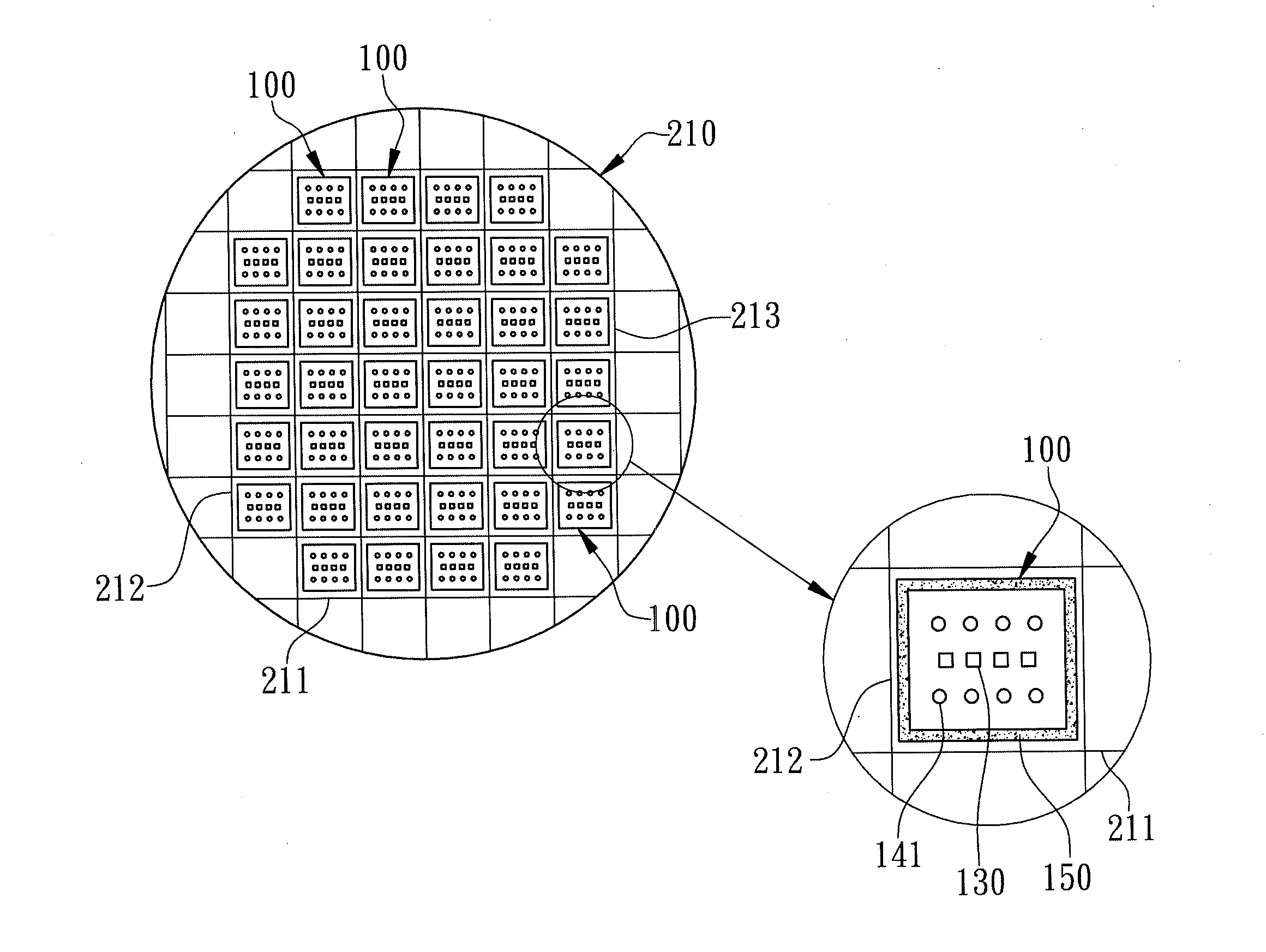
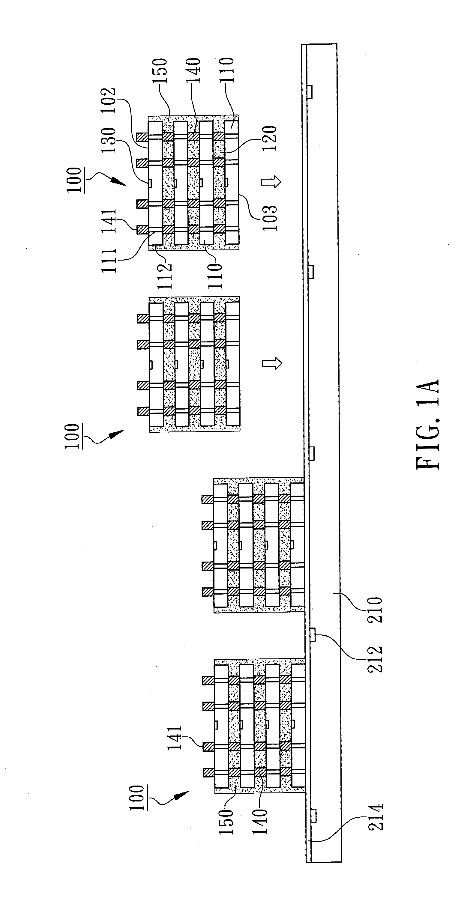
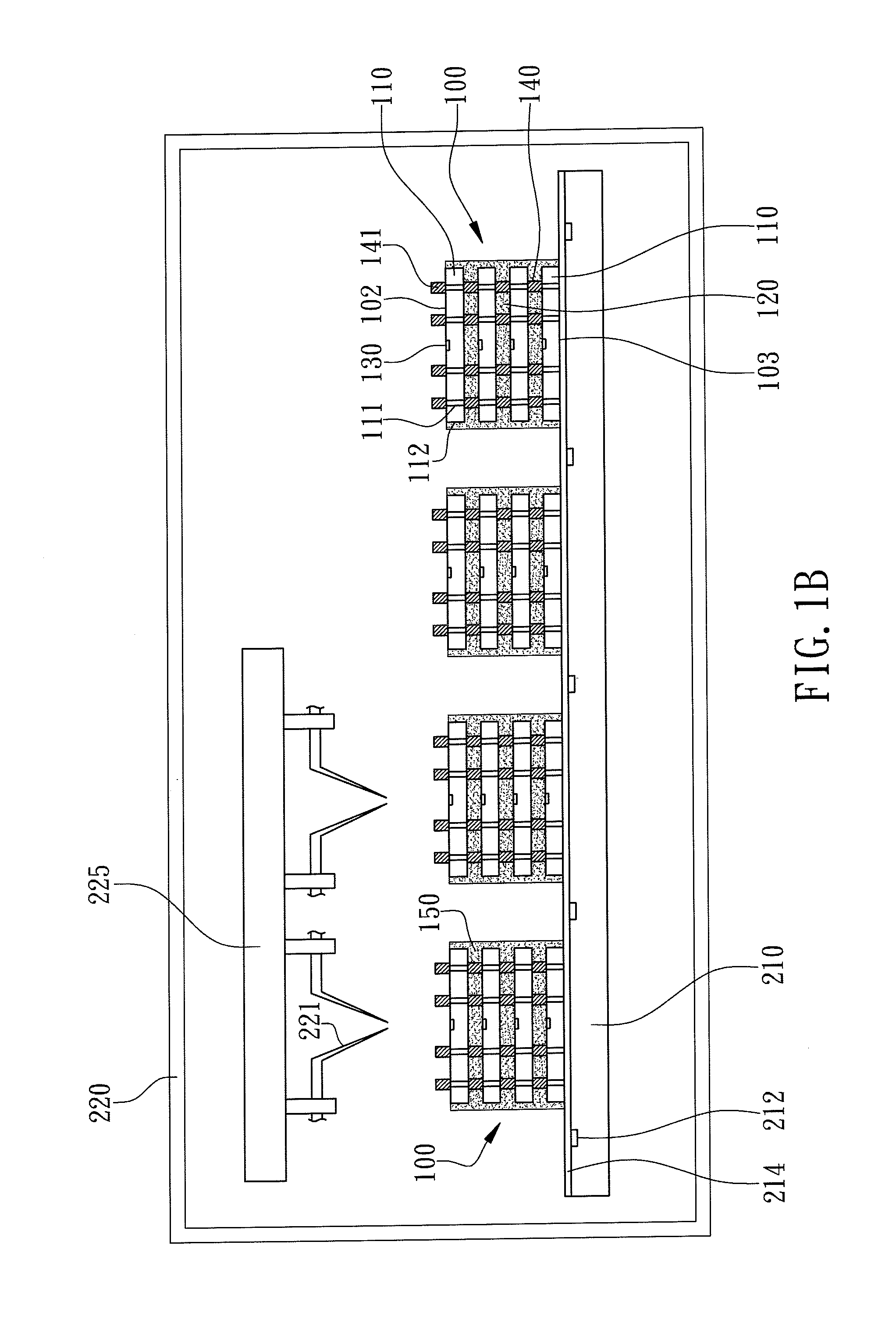
[0014]With reference to the attached drawings, the present invention is described by means of the embodiment(s) below where the attached drawings are simplified for illustration purposes only to illustrate the structures or methods of the present invention by describing the relationships between the components and assembly in the present invention. Therefore, the components shown in the figures are not expressed with the actual numbers, actual shapes, actual dimensions, nor with the actual ratio. Some of the dimensions or dimension ratios have been enlarged or simplified to provide a better illustration. The actual numbers, actual shapes, or actual dimension ratios can be selectively designed and disposed and the detail component layouts may be more complicated.

[0015]According to the preferred embodiment of the present invention, the method for wafer-level testing a plurality of diced multi-chip stacked packages is illustrating from FIG. 1A to FIG. 1E for component cross-sectional v...


PUM


Abstract

Disclosed is a method for wafer-level testing a plurality of diced multi-chip stacked packages. Each package includes a plurality of chips with vertically electrical connections such as TSVs. Next, according to a die-on-wafer array arrangement, the multi-chip stacked packages are fixed on a transparent reconstructed wafer by a photo-sensitive adhesive, and the packages are located within the component-bonding area of the wafer. Then, the transparent reconstructed wafer carrying the multi-chip stacked packages can be loaded into a wafer tester for probing. Accordingly, the wafer testing probers in the wafer tester can be utilized to probe the testing electrodes of the stacked packages so that it is easy to integrate this wafer-level testing method especially into TSV packaging processes.

Description

FIELD OF THE INVENTION[0001]The present invention relates to a manufacture method of semiconductor devices and more specifically to a method for wafer-level testing a plurality of diced multi-chip stacked packages.BACKGROUND OF THE INVENTION[0002]Multi-chip packages are high-density packaging technology, i.e., a plurality of vertically stacked chips are packaged inside a package. The current methodology is to stack chips one by one on a wiring substrate and then packaging and testing through the wiring substrate, however, the footprint and the package thickness are increased.[0003]In order to reduce the package dimension of a multi-chip package, conventionally substrates were eliminated by vertically stacking a plurality of wafers in wafer form, then the stacked wafers were singluated into substrate-less multi-chip packages or called “dice cube”, one of relative technologies is disclosed in US Patent No. 2011 / 0074017 taught by MORIFUJI et al. However, bad chips were inevitably exist...

Claims


Application Information

Patent Timeline
Patent Type & Authority Applications(United States)
IPC IPC(8): H01L21/66
CPCH01L22/14H01L22/20H01L2224/16145H01L2224/73204H01L2225/06513H01L2225/06541H01L25/50H01L25/0657
Inventor KAI-JUN, CHANGYU-SHIN, LIUSHIN-KUNG, CHENKUN-CHIH, CHAN
Owner POWERTECH TECHNOLOGY
Learn More