Active matrix organic light-emitting diode panel packaging structure

Inactive Publication Date: 2014-02-27
TCL CHINA STAR OPTOELECTRONICS TECH CO LTD +1
View PDF3 Cites 1 Cited by
  • Summary
  • Abstract
  • Description
  • Claims
  • Application Information

AI Technical Summary

Benefits of technology

The present invention provides an active matrix organic light-emitting diode panel packaging structure that is excellent in both sealability and bondability, and helps in realizing the size enlargement of the panel. The structure includes a loop of organic bonding material that surrounds the pixel zone, which overcomes the issue of poor bondability for large-sized panels. The separate arrangement of organic bonding material and inorganic packaging material helps keeping the individual performance and not mutually affecting each other, thereby possessing both advantages of excellent packaging sealability and bondability.

Problems solved by technology

However, since glass cement is rigid, although it could effectively block humidity and oxygen, yet the bonding property is poor.
Thus, to achieve size enlargement for AMOLED panels, the bonding property for jointing a substrate and a back lid is a severe challenge for glass cement.

Method used


Image

  • Active matrix organic light-emitting diode panel packaging structure
  • Active matrix organic light-emitting diode panel packaging structure
  • Active matrix organic light-emitting diode panel packaging structure

Examples


Embodiment Construction

[0040]To further expound the technical solution adopted in the present invention and the advantages thereof, a detailed description is given to a preferred embodiment of the present invention and the attached drawings.

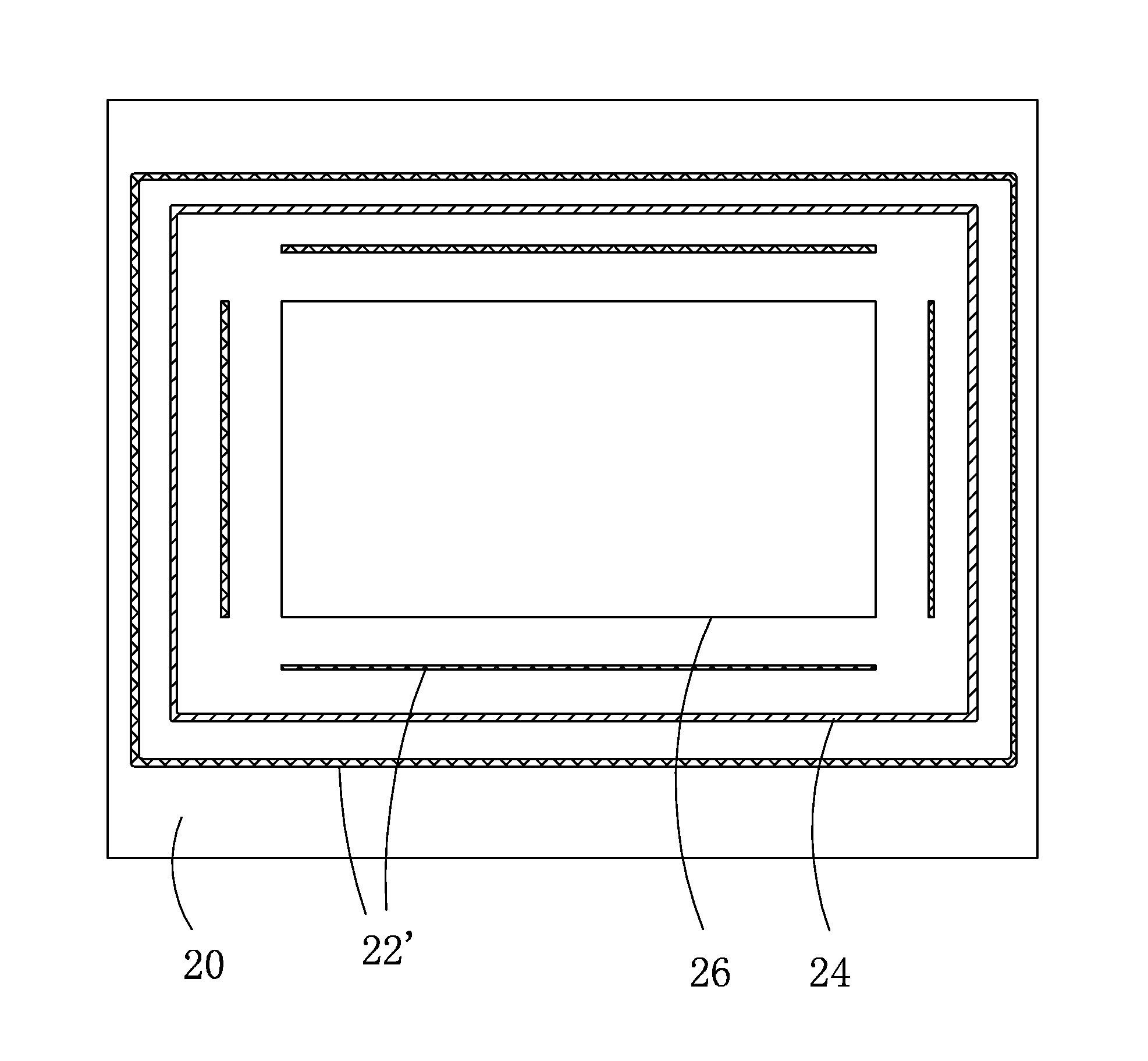
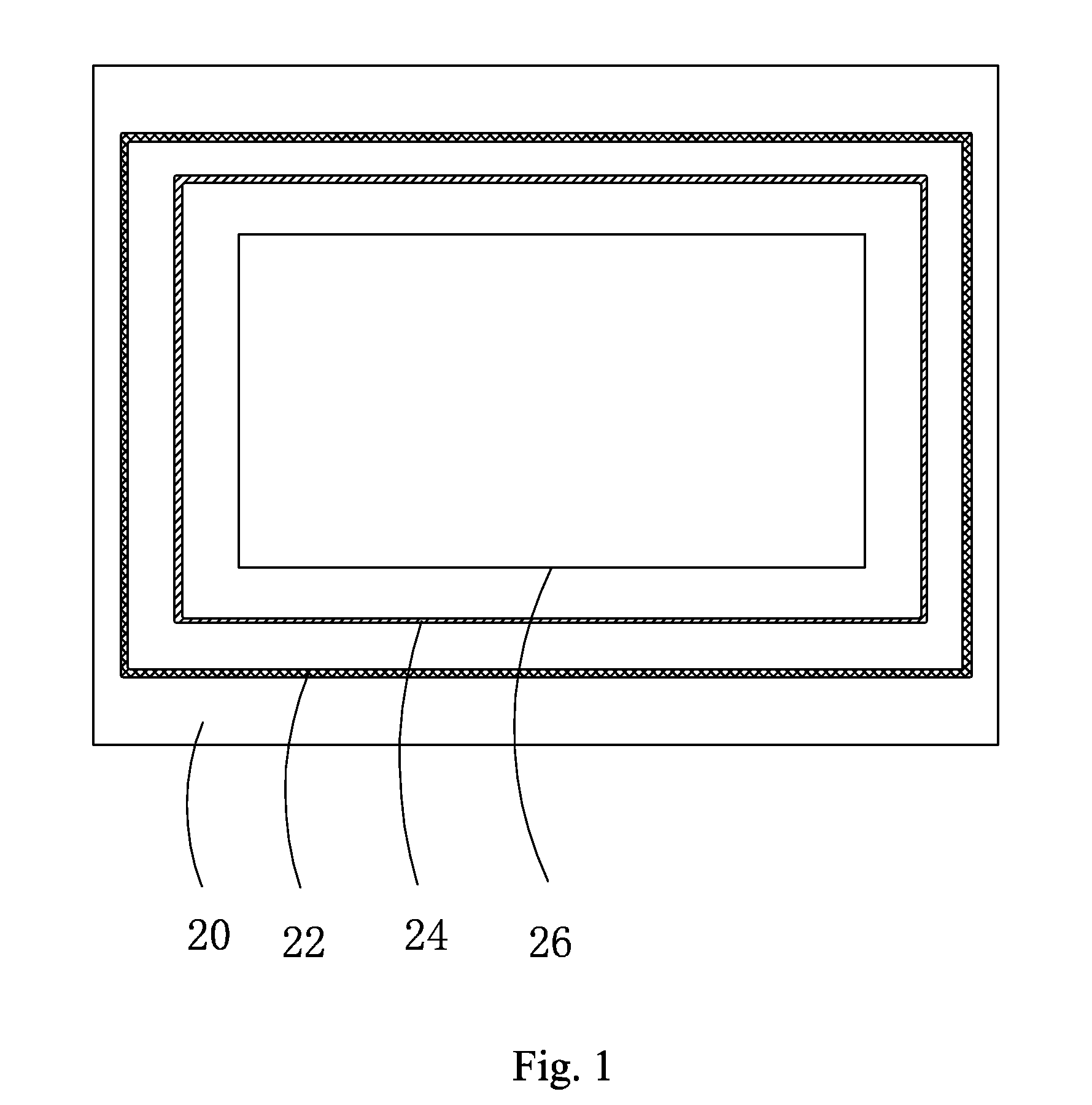
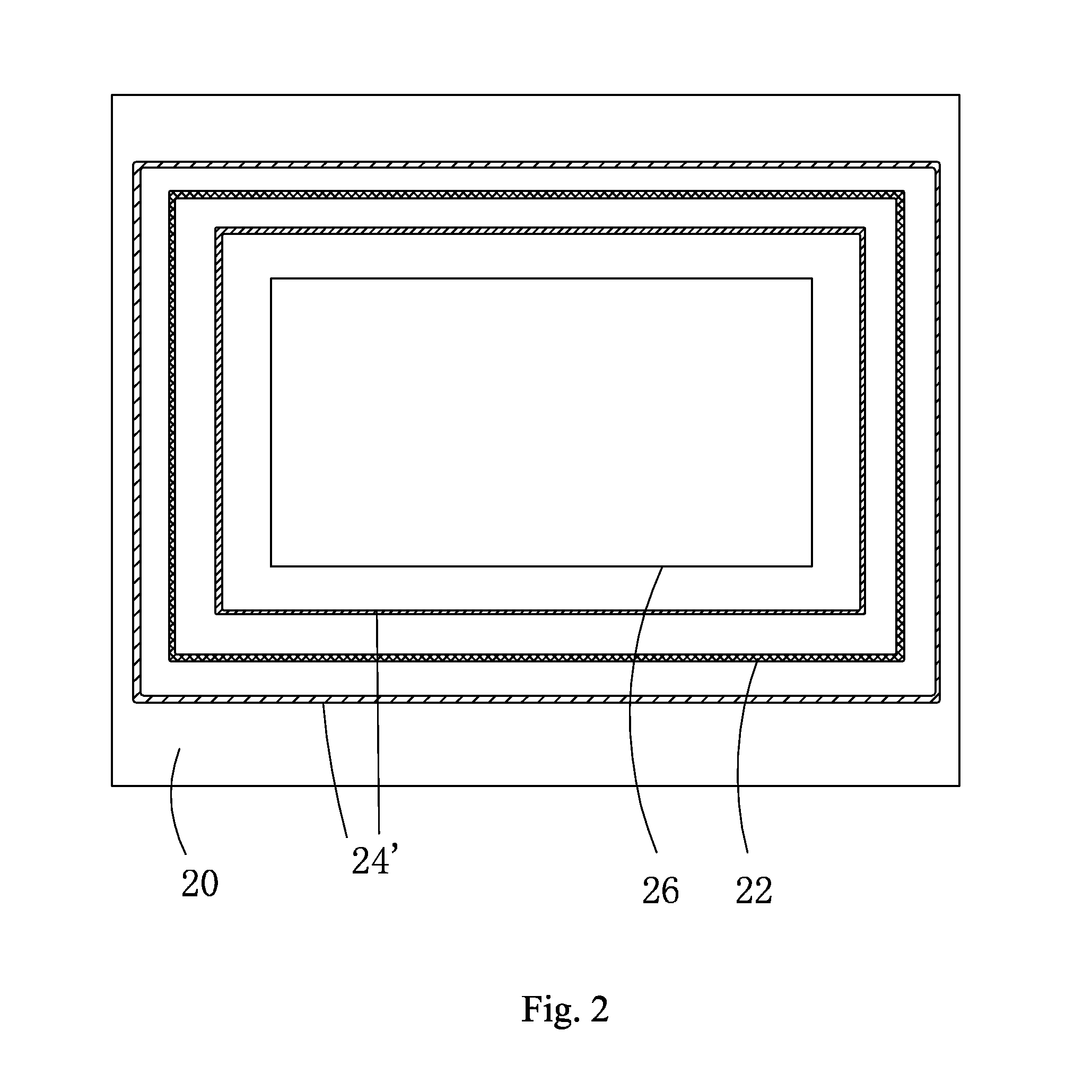
[0041]Referring to FIG. 1, the present invention provides an active matrix organic light-emitting diode (AMOLED) panel packaging structure, which comprises a substrate 20, a pixel zone 26 formed on the substrate 20, multiple loops of inorganic packaging material 24 formed on the substrate 20 and located outside the pixel zone 26, multiple loops of organic bonding material 22 formed on the substrate 20 and located outside the pixel zone 26, and a back lid (not shown) covering over the inorganic packaging material 24 and the organic bonding material 22. The multiple loops of inorganic packaging material 24 include at least one loop that circumferentially and hermetically surrounds the pixel zone 26. The multiple loops of organic bonding material 22 include at least one l...


PUM


Abstract

The present invention provides an active matrix organic light-emitting diode (AMOLED) panel packaging structure, which includes a substrate, a pixel zone formed on the substrate, multiple loops of inorganic packaging material formed on the substrate and located outside the pixel zone, multiple loops of organic bonding material formed on the substrate and located outside the pixel zone, and a back lid covering over the inorganic packaging material and the organic bonding material. The multiple loops of inorganic packaging material include at least one loop that circumferentially and hermetically surrounds the pixel zone. The multiple loops of organic bonding material include at least one loop that circumferentially and hermetically surrounds the pixel zone. The inorganic packaging material and the organic bonding material are arranged to separate from each other. The AMOLED panel packaging structure possesses advantages of excellent packaging sealability and bondability and helps realization of size enlargement of AMOLED panel.

Description

BACKGROUND OF THE INVENTION[0001]1. Field of the Invention[0002]The present invention relates to the field of organic light-emitting diode, and in particular to an active matrix organic light-emitting diode panel packaging structure.[0003]2. The Related Arts[0004]OLED (Organic Light-Emitting Diode) is luminescence caused by injection and recombination of carriers when an organic semiconductor material and luminescent material is driven by an electric field. Luminescence of OLED is achieved by using an ITO transparent electrode and a metal electrode as anode and cathode of a device by which a predetermined voltage is applied to drive electrons and electron holes that are injected through the cathode and the anode into electron and hole transportation layers and migrate from the electron and hole transportation layers to a luminescent layer where the electrons and the holes meet each other to form excitons and excite luminescent molecules. The later, after radiative relaxation, gives ...

Claims


Application Information

Patent Timeline
IPC IPC(8): H01L27/32
CPCH01L27/3244H10K59/12H10K59/8722H10K50/8426
Inventor LIU, CHIHCHE
Owner TCL CHINA STAR OPTOELECTRONICS TECH CO LTD
Why Eureka
Try Eureka