Control Circuit, Time Calculating Unit, and Operating Method for Control Circuit
Active Publication Date: 2014-02-27
UPI SEMICON CORP
13 Cites 2 Cited by
AI-Extracted Technical Summary
Problems solved by technology
When a designer designs this system, he/she can determine the width magnification of the pulse signal; however, in practical applications, this default magnification is fixed instead of being dynamically adjusted with different loads, therefore, it lacks of flexibility to use.
In addition, the switching between 1 ...
Method used
[0033]By doing so, the control circuit 3 can speed up the transient response speed to the load 4 and dynamically adjust the on-time (namely the pulse width) of the corresponding switch conducting signal Ton to W1˜W5 according to the differences ΔV1˜ΔV5 between the control signal Vcon and the reference voltage Vref. Therefore, it can adapt any load 4 changing situations to effectively improve the drawbacks of the prior arts including that the fixed pulse magnification used in the prior arts is failed to be dynamically adjusted with different loads and that it is hard to accurately determine when to start to output the switch conducting signal Ton or to stop outputting the switch conducting signal Ton.
[0039]Compared to the prior arts, the control circuit, time calculating unit, and contr...
Benefits of technology
[0007]A scope of the invention is to provide a control circuit. In a preferred embodiment, the control circuit is operated in a power converter and coupled to a load. The control circuit includes an output stage and a time calculating unit. The time calculating unit is coupled to the output stage. The time calculating unit is used for receiving a control signal and a refe...
Abstract
A control circuit, a time calculating unit, and operating method for control circuit are disclosed. The control circuit is operated in a power converter and coupled to a load. The control circuit includes an output stage and a time calculating unit. The time calculating unit receives a control signal and a reference voltage and provides a switch conducting signal to the output stage. The generation of the control signal is related to an output voltage of the power converter. When the difference between the control signal and the reference voltage becomes larger due to the change of the load, the time calculating unit dynamically increases an on-time of the switch conducting signal.
Application Domain
Efficient power electronics conversionDc-dc conversion +2
Technology Topic
Voltage referenceEngineering +2
Image
Examples
- Experimental program(1)
Example
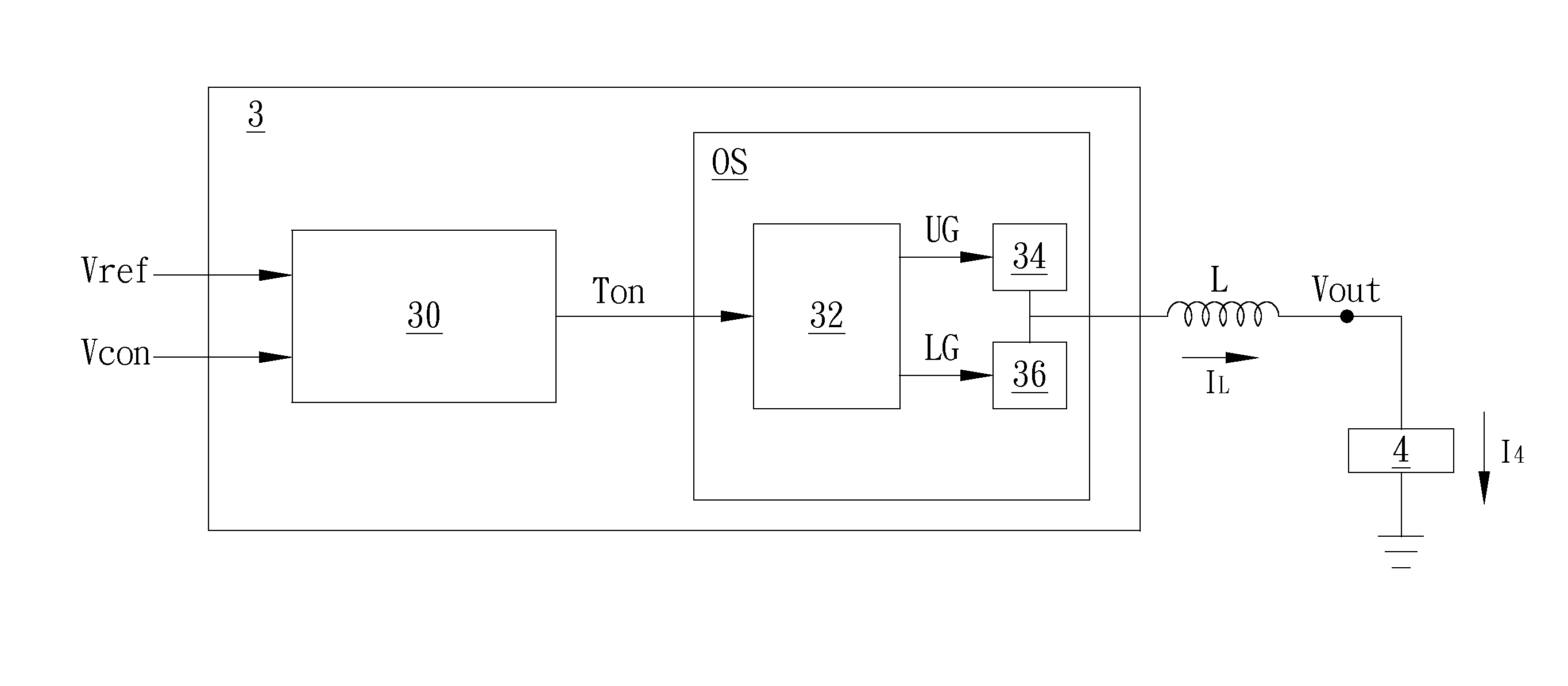
[0022]A preferred embodiment of the invention is a control circuit operated in a power converter. In fact, the control circuit of the embodiment of the invention can be applied to a fixed frequency DC-DC converter or a constant-on-time (COT) DC-DC converter, but not limited to these. The control circuit of the invention can be applied to other power converter circuit structures, such as an AC-DC converter or a Dc-AC converter.
[0023]At first, please refer to FIG. 3. FIG. 3 illustrates a circuit structure schematic diagram of the control circuit operated in the power converter of this embodiment. As shown in FIG. 3, the control circuit 3 is coupled to a load 4 via the output inductor L. The control circuit 3 includes an output stage OS and a time calculating unit 30. The time calculating unit 30 is coupled to the output stage OS. The time calculating unit 30 receives a control signal Vcon and a reference voltage Vref and selectively provides a switch conducting signal Ton to the output stage OS according to the control signal Vcon and the reference voltage Vref. The output stage OS includes a driver 32, a first switch 34, and a second switch 36. The output stage OS is coupled to the load 4 through an output inductor L. The driver 32 outputs switch conducting signals UG and LG to the first switch 34 and the second switch 36 respectively to switch the first switch 34 and the second switch 36 on. The current flowing through the output inductor L is an output inductor current IL; the current flowing through the load 4 is a load current I4; the voltage between the output inductor L and the load 4 is an output voltage Vout of the power converter.
[0024]FIG. 4 illustrates a circuit structure schematic diagram of the time calculating unit 30 shown in FIG. 3. As shown in FIG. 4, the time calculating unit 30 includes a first current source Iton, a first transistor MP1, a second transistor MP2, an operational amplifier OP1, a comparator OP2, a charging capacitor C1, and a charging switch SW1. The first current source Iton is coupled between the first transistor MP1 and a ground terminal; the first transistor MP1 and the second transistor MP2 are coupled relative to each other to form a current mirror; the charging capacitor C1 is coupled between the second transistor MP2 and the ground terminal; two terminals of the charging switch SW1 are coupled to two sides of the charging capacitor C1; the operational amplifier OP1 and the comparator OP2 are coupled to a node between the second transistor MP2 and the charging capacitor Cl.
[0025]The first current source Iton is a function of the input voltage Vin of the power converter. That to say, the first current source Iton provides a first current mI to charge the charging capacitor C1 through the current mirror formed by the first transistor MP1 and the second transistor MP2. At this time, the charging switch SW1 is open, so that the first current mI can flow to the charging capacitor C1 to charge the charging capacitor C1. The comparator OP2 compares the charging voltage Vc of the charging capacitor C1 with the output voltage Vout of the power converter. When the charging capacitor C1 is charged and the charging voltage Vc of the charging capacitor C1 is higher than the output voltage Vout of the power converter, namely the comparison result obtained by the comparator OP2 is that the charging voltage Vc is higher than the output voltage Vout, it means that the charging process is done, the comparator OP2 will stop outputting the switch conducting signal Ton to the output stage OS, and the charging switch SW1 will be switched on to make the first current mI flow to the ground terminal through the charging switch SW1 to stop the first current mI charging the charging capacitor C1.
[0026]In this embodiment, since the operational amplifier OP1 receives two voltage signals (the control signal Vcon and the reference voltage Vref) and selectively generates a second current source nI according to the control signal Vcon and the reference voltage Vref, the operational amplifier OP1 is a voltage-to-current circuit device. The operational amplifier OP1 compares the control signal Vcon with the reference voltage Vref and calculates a difference between the control signal Vcon and the reference voltage Vref. In fact, the control signal Vcon can be an error signal (comp) obtained by comparing the output voltage Vout of the power converter with a default voltage or a feedback signal (Vfb) related to the output voltage Vout of the power converter, but not limited to these.
[0027]When the comparison result obtained by the operational amplifier OP1 is that the control signal Vcon is smaller than or equal to the reference voltage Vref, the operational amplifier OP1 will not generate the second current source nI, namely the second current I2 of the second current source nI is 0. At this time, the charging current I1 flowing through the charging capacitor C1 equals to the first current mI.
[0028]When the comparison result obtained by the operational amplifier OP1 is that the control signal Vcon is larger than the reference voltage Vref, the operational amplifier OP1 will start to generate the second current source nI, namely the second current I2 of the second current source nI is larger than 0. At this time, the second current I2 is a part of the first current mI flowing toward the second current source nI. That is to say, the first current mI equals to a sum of the second current I2 and the charging current I1. Therefore, the charging current I1 flowing through the charging capacitor C1 is smaller than the first current mI.
[0029]Because the reference voltage Vref is a fixed value, once the control signal Vcon becomes larger, the difference between the control signal Vcon and the reference voltage Vref will also become larger accordingly. The operational amplifier OP1 will adjust the second current I2 of the second current source nI according to the difference between the control signal Vcon and the reference voltage Vref. When the difference between the control signal Vcon and the reference voltage Vref becomes larger, the second current I2 of the second current source nI generated by the operational amplifier OP1 will also become larger and the charging current I1 charging to the charging capacitor C1 will become smaller, so that the time needed for the charging current I1 to charge the charging capacitor C1 to the charging voltage Vc higher than the output voltage Vout of the power converter will become longer. Therefore, the on-time from the time to start to output the switch conducting signal Ton to the output stage OS to the time to stop outputting the switch conducting signal Ton to the output stage OS becomes longer (namely the pulse width of the switch conducting signal Ton becomes larger).
[0030]FIG. 5 illustrates timing diagrams of the signals when the load 4 becomes heavy-loaded from light-loaded. As shown in FIG. 5, when the load 4 generates transient change at time t1 (namely the load 4 becomes heavy-loaded from light-loaded), the load current I4 and the output inductor current IL will be changed from the low-level to the high-level, so that the output voltage Vout of the power converter will be increased and the control signal Vcon related to the output voltage Vout will be also increased accordingly. Once the control signal Vcon is larger than the reference voltage Vref, the operational amplifier OP1 will generate the second current I2 of the second current source nI according to the difference between the control signal Vcon and the reference voltage Vref, so that the charging current I1 flowing through the charging capacitor C1 is smaller than the first current mI. Therefore, the time needed for the charging current I1 to charge the charging capacitor C1 to the charging voltage Vc higher than the output voltage Vout of the power converter becomes longer; that is to say, the on-time of the switch conducting signal Ton becomes longer.
[0031]During the period of the time t1 to the time t2, the control signal Vcon is increased to over the reference voltage Vref, the operational amplifier OP1 will generate the second current I2 of the second current source nI and linearly adjust the second current I2 of the second current source nI according to the difference between the control signal Vcon and the reference voltage Vref to linearly adjust the on-time of the switch conducting signal Ton (namely the pulse width of the switch conducting signal Ton).
[0032]After the control signal Vcon is increased to over the reference voltage Vref, if the control signal Vcon is continuously increased, the difference between the control signal Vcon and the reference voltage Vref is gradually increased from 0 to ΔV4; therefore, the on-time (namely the pulse width) of the corresponding switch conducting signal Ton is also increased from W to W4. When the control signal Vcon is decreased, the difference between the control signal Vcon and the reference voltage Vref will be decreased from ΔV4 to ΔV5. Therefore, the on-time (namely the pulse width) of the corresponding switch conducting signal Ton is also decreased from W4 to W5.
[0033]By doing so, the control circuit 3 can speed up the transient response speed to the load 4 and dynamically adjust the on-time (namely the pulse width) of the corresponding switch conducting signal Ton to W1˜W5 according to the differences ΔV1˜ΔV5 between the control signal Vcon and the reference voltage Vref. Therefore, it can adapt any load 4 changing situations to effectively improve the drawbacks of the prior arts including that the fixed pulse magnification used in the prior arts is failed to be dynamically adjusted with different loads and that it is hard to accurately determine when to start to output the switch conducting signal Ton or to stop outputting the switch conducting signal Ton.
[0034]Another preferred embodiment of the invention is an operating method for a control circuit. In this embodiment, the control circuit is operated in a power converter and coupled to a load. The control circuit includes an output stage. Please refer to FIG. 6. FIG. 6 illustrates a flowchart of the operating method for the control circuit in this embodiment.
[0035]As shown in FIG. 6, at first, the method performs the step S10 to receive a control signal and a reference voltage and provide a switch conducting signal to the output stage, wherein the control signal is generated related to an output voltage of the power converter. In fact, the control signal can be an error signal obtained by comparing the output voltage of the power converter with a reference voltage or a feedback signal related to the output voltage of the power converter, but not limited to this.
[0036]Next, the method performs the step S12 to determine whether the control signal is larger than the reference voltage. If the determining result of the step S12 is yes, it means that the control signal is increased over the fixed reference voltage; therefore, the method will perform the step S14 to generate a second current source and the step S16 to dynamically adjust a second current of the second current source according to a difference between the control signal and the reference voltage. When the loading becomes heavy-loaded from light-loaded, the output voltage of the power converter will be increased and the control signal related to the output voltage of the power converter will be also increased, so that the difference between the control signal and the reference voltage will be increased. Therefore, the method dynamically increases the second current of the second current source according to the increased difference between the control signal and the reference voltage
[0037]Then, the method performs the step S18 to determine whether the charging voltage of the charging capacitor is higher than the output voltage of the power converter. If the determining result of the step S18 is yes, it means that the charging capacitor has been charged by the charging current to the charging voltage higher than the output voltage of the power converter. Therefore, the method performs the step S20 to stop outputting the switch conducting signal to the output stage.
[0038]It should be noticed that when the load becomes heavy-loaded from light-loaded, the second current of the second current source becomes larger and the charging current flowing through the charging capacitor becomes smaller, so that the time needed for the charging current to charge the charging capacitor to the charging voltage higher than the output voltage of the power converter becomes longer. Therefore, the on-time from the time to start to output the switch conducting signal to the output stage to the time to stop outputting the switch conducting signal to the output stage becomes longer (namely the pulse width of the switch conducting signal becomes larger).
[0039]Compared to the prior arts, the control circuit, time calculating unit, and control circuit operating method operated in the power converter of the invention dynamically adjusts the on-time of the switch conducting signal in a linear way according to the variation of the load. Therefore, when the load becomes heavy-loaded from light-loaded, the transient response speed to the load will be faster and any load changing situations can be adapted. Furthermore, compared to the digital dichotomy used in the conventional power converter, it is more accurate that the power converter of the invention uses analog amplifier to determine how to change the on-time of the switch conducting signal (the width of the pulse signal). During the load transient changing process, the on-time of the switch conducting signal is still controlled by the loop to maintain the system stability.
[0040]With the example and explanations above, the features and spirits of the invention will be hopefully well described. Those skilled in the art will readily observe that numerous modifications and alterations of the device may be made while retaining the teaching of the invention. Accordingly, the above disclosure should be construed as limited only by the metes and bounds of the appended claims.
PUM


Description & Claims & Application Information
We can also present the details of the Description, Claims and Application information to help users get a comprehensive understanding of the technical details of the patent, such as background art, summary of invention, brief description of drawings, description of embodiments, and other original content. On the other hand, users can also determine the specific scope of protection of the technology through the list of claims; as well as understand the changes in the life cycle of the technology with the presentation of the patent timeline. Login to view more.