Microfluidic device and method of fabricating microfluidic devices

a microfluidic device and microfluidic technology, applied in the field of microchannels for microfluidic devices, can solve the problems of difficult surface masking control, plastics are less desirable in such applications, and the bond between the substrate having the recess and the overlying cover material is difficult to achiev

Inactive Publication Date: 2014-03-06
NASA
View PDF6 Cites 15 Cited by
  • Summary
  • Abstract
  • Description
  • Claims
  • Application Information

AI Technical Summary

Benefits of technology

[0012]As described herein, the exemplary embodiments overcome one or more of the above or other disadvantages known in the art.

Problems solved by technology

Plastics are less desirable in such applications, plastics tending to leach organics into fluids contacting the structure.
Each of these techniques pose challenges to fabricating microfluidic devices, the first being difficult to control with surface masking, and the second tending to leave unusual contours in the recess cross-section which influence the usual fluid mechanics associated in manipulating small fluid volumes.
Another problem with conventional methods of fabricating LOC microstructures is the bond between the substrate having the recess and the overlying cover material.
Such chips are therefore unsuitable for applications where extremely high micro-channel pressures are expected, such as in-situ planetary exploration, where pressures of 276 bar (4,000 psi) are expected.
Yet another problem with conventional methods of fabricating chip microstructures is the resulting channel shape.
Similarly, conventional etching techniques typically result in micro-channels with square cross-sections.
Flat surfaces and square cross-sections induce turbulences into fluid flow which may change the optical properties of the fluid, posing challenges to optical analysis techniques such as spectroscopy.

Method used


Image

  • Microfluidic device and method of fabricating microfluidic devices
  • Microfluidic device and method of fabricating microfluidic devices
  • Microfluidic device and method of fabricating microfluidic devices

Examples


Embodiment Construction

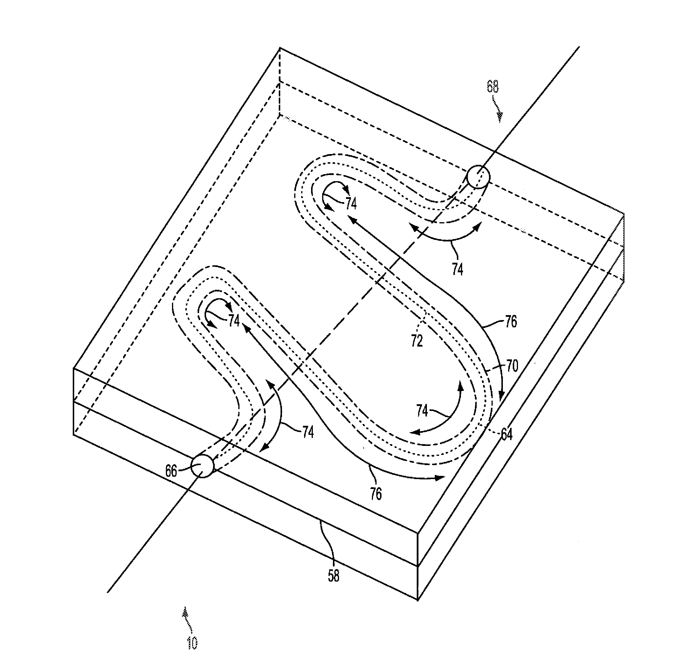
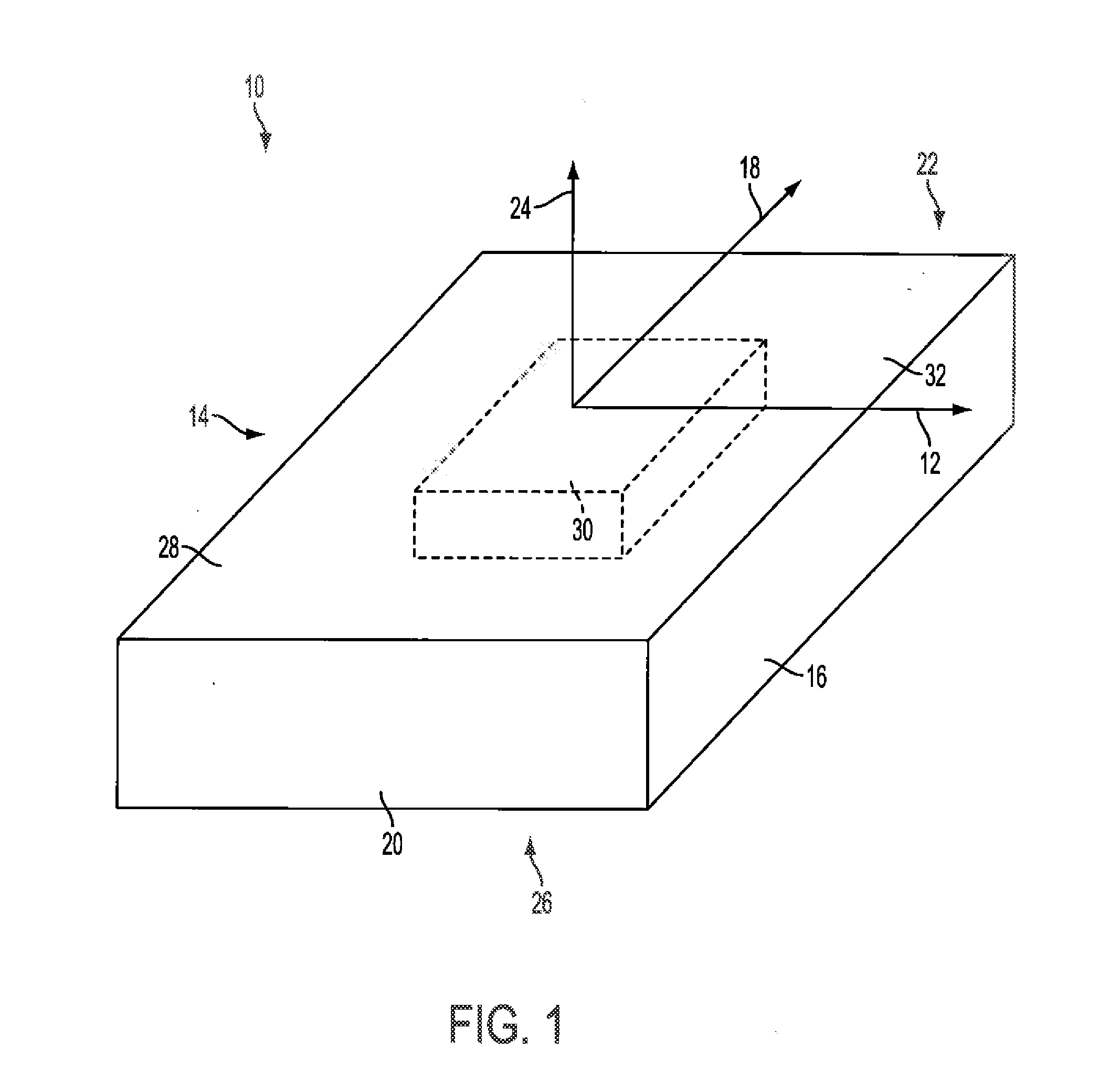
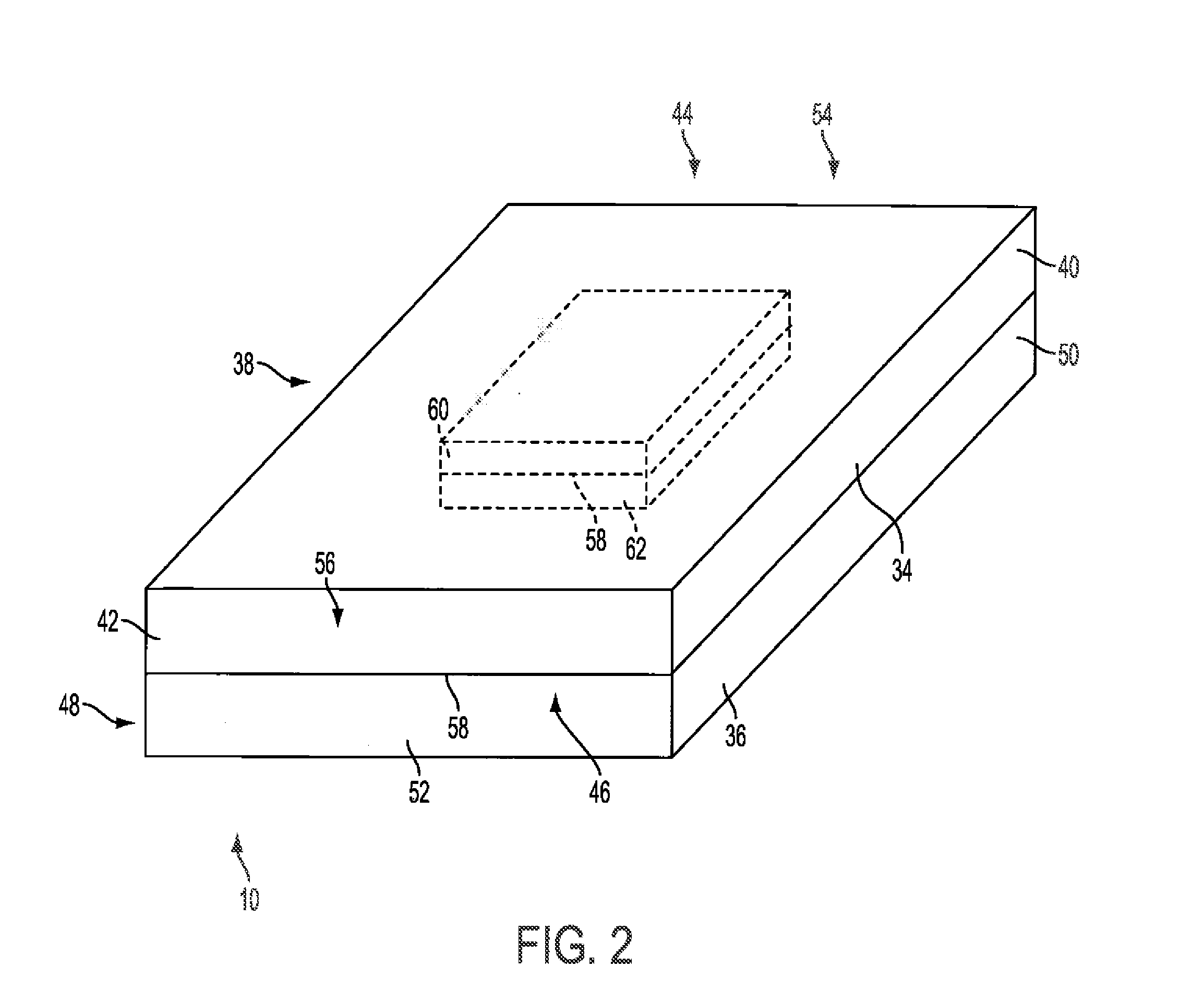
[0027]Detailed illustrative embodiments of example embodiments are disclosed herein. However, specific structural and functional details disclosed herein are merely representative for purposes of describing example embodiments. The example embodiments may, however, be embodied in many alternate forms and should not be construed as limited to only example embodiments set forth herein.

[0028]As used herein, the terms “front,”“rear,”“left,”“right,”“top,”“bottom,”“upper,” and “lower” refer to relative placement of features shown in the drawings. These terms do not indicate that any specific embodiment is limited in its orientation unless otherwise specified in the accompanying description. As used herein, the terms “first” and “second” are used to distinguish one element from another and do not refer to any particular order or positional relationship. For example, a first element could be termed a second element, and, similarly, a second element could be termed a first element, without d...


PUM


Abstract

Lab-on-a-chip microfluidic devices having micro-channels able to withstand an internal channel pressure of more than 4,000 psi are described. The micro-channels have rounded cross-sections that prevent turbulent flow within a fluid conveyed within the channel. The channel may have serpentine-shaped length extending between a channel inlet and a channel outlet, the channel thereby being of sufficient length to observe both the stationary and moving phases of the fluid in a chip having a sufficiently small footprint that it is suitable for incorporation into a miniaturized spectrometer. Methods of fabricating lab-on-a-chip microfluidic devices are described by etching recesses in chip substrates such that a first substrate recess mirrors a second substrate recess in an opposed orientation, aligning the substrates such the recesses cooperatively define a micro-channel having a rounded cross-section, and bonding the substrates to define a smooth-walled micro-channel.

Description

GOVERNMENT INTERESTS[0001]The subject matter described herein was made in the performance of work under a NASA contract and by employees of the United States Government. As such, the subject matter disclosed herein is subject is subject to the provisions of Public Law 96-517 as codified in 35 U.S.C. §202, and may be manufactured and used by or for the Government for governmental purposes without the payment of any royalties thereon or therefore.BACKGROUND[0002]1. Field[0003]The aspects of the present disclosure relate generally to micro-channels for microfluidic devices. More specifically, the aspects of the present disclosure relate to a lab-on-a-chip analytical device having at least one micro-channel and methods for manufacturing such devices.[0004]2. Description of Related Art[0005]A lab-on-a-chip (LOC) is a microfluidic device used for studying a fluid conveyed within the chip. They typically contain microstructures, such as micro-channels, pumps, valves, reservoirs, mixers, an...

Claims


Application Information

Patent Timeline
Patent Type & Authority Applications(United States)
IPC IPC(8): B01L3/00
CPCB01L3/502707B01L3/502746B01L3/569B01L2200/027B01L2200/0689B01L2300/0816B01L2300/0883B01L2300/0887B01L2300/12G01N30/6095Y10T156/1052
Inventor ZHENG, YUNWASSELL, EDWARDBALVIN, MANUELGETIY, STEPHANIE
Owner NASA
Why Eureka
Try Eureka