Solid-state image sensor

a solid-state image and sensor technology, applied in the field of solid-state image sensors, can solve the problems of reducing the optical efficiency of the camera, the decrease of the optical efficiency of the color filter, and the intensity of the light falling on a single pixel, so as to increase the number of photosensitive cells to use, high optical efficiency, and high color reproducibility

Inactive Publication Date: 2014-03-20
SOVEREIGN PEAK VENTURES LLC
View PDF3 Cites 19 Cited by
  • Summary
  • Abstract
  • Description
  • Claims
  • Application Information

AI Technical Summary

Benefits of technology

[0025]According to an aspect of the present invention, a dispersive element that makes an incoming light ray incident on any of multiple different photosensitive cells is used according to its color component. As a result, even if crosstalk between the light rays being

Problems solved by technology

Nevertheless, the greater the number of pixels in an image sensor, the lower the intensity of the light falling on a single pixel and the lower the sensitivity of camera tends to be.
That is why with such a color filter, the optical efficiency of a camera would decrease.
It is true that the aperture ratio can be increased substantially by this technique but the decrease in optical efficiency by color filters still persists.
As a r

Method used


Image

  • Solid-state image sensor
  • Solid-state image sensor
  • Solid-state image sensor

Examples


embodiment 1

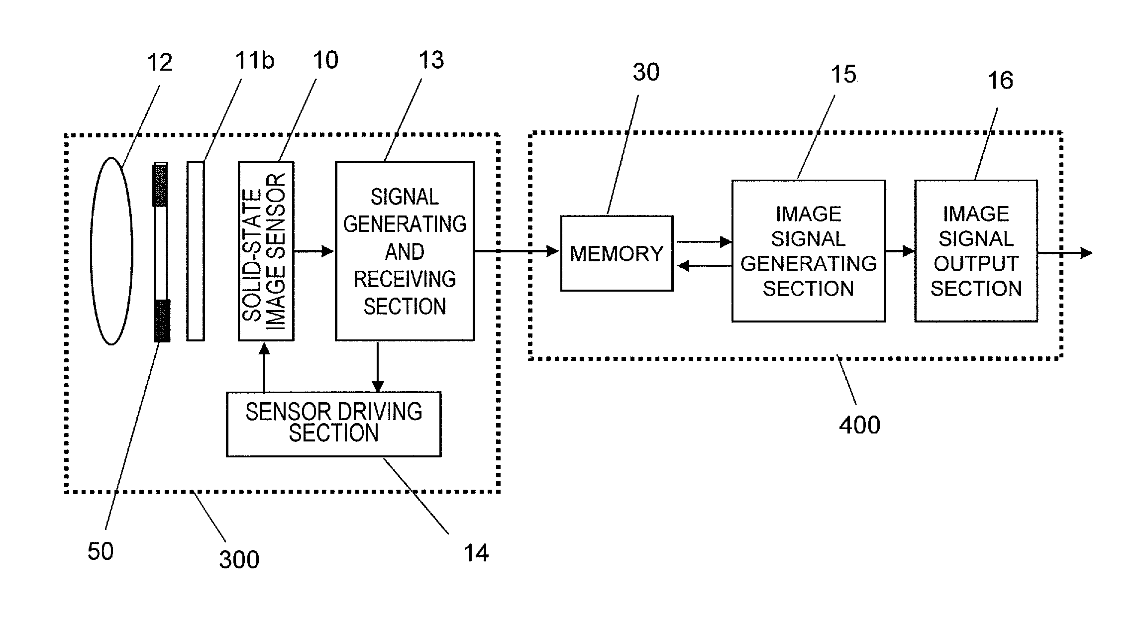
[0092]FIG. 3 is a block diagram illustrating an overall configuration for an image capture device as a first embodiment. The image capture device of this embodiment is a digital electronic camera and includes an image capturing section 300 and a signal processing section 400 that receives a signal from the image capturing section 300 and outputs a signal representing an image (i.e., an image signal). The image capture device may either generate only a still picture or have the function of generating a moving picture.

[0093]The image capturing section 300 includes an optical lens 12 which images a given subject, an optical diaphragm 50, an optical filter 11b, and a solid-state image sensor 10 (which will be simply referred to herein as an “image sensor”) which converts the optical information that has been gotten through the optical lens 12 and the optical filter 11b into an electrical signal by photoelectric conversion. The image capturing section 300 further includes a signal genera...

embodiment 2

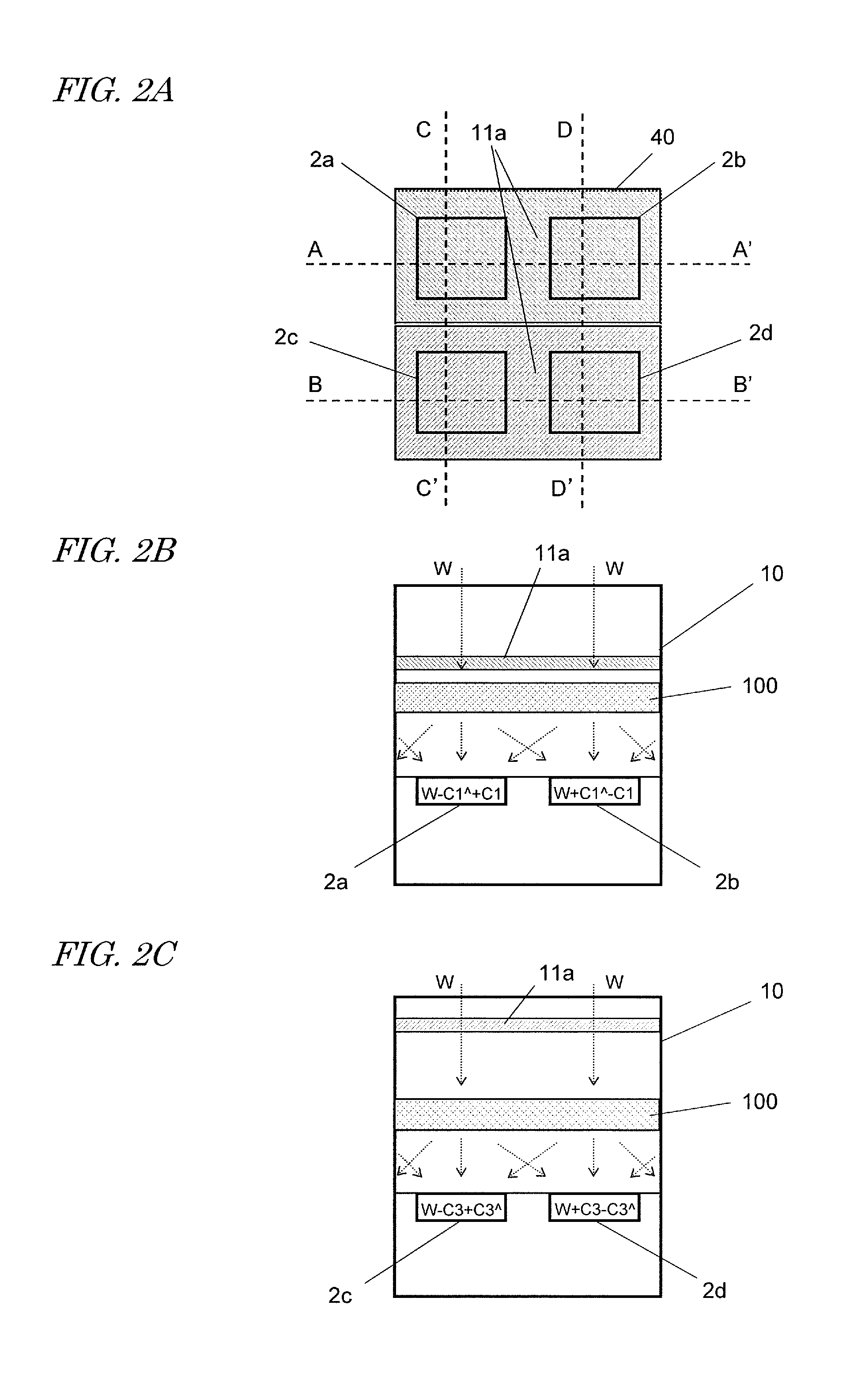
[0126]Next, a second embodiment will be described with reference to FIGS. 8A through 8D. In an image capture device according to this embodiment, its image sensor 10 has dispersive elements with a different configuration, and performs signal processing in a different way, from in the image capture device of the first embodiment. But other than that, quite the same members are used in both of the first and second embodiments. That is why the following description of this second embodiment will be focused on only the differences from the image capture device of the first embodiment, and their common features will not be described all over again to avoid redundancies.

[0127]FIG. 8A illustrates a basic configuration for an image sensor 10 according to this embodiment. FIGS. 8B and 8C are cross-sectional views as respectively viewed on the planes C-C′ and D-D′ shown in FIG. 8A. The dispersive elements of the image sensor 10 of this embodiment are configured as shown in FIGS. 8A through 8C...


PUM


Abstract

This solid-state image sensor includes an array of photosensitive cells and an array of dispersive elements. The photosensitive cell array is comprised of a plurality of unit blocks 40, each including four photosensitive cells 2a, 2b, 2c and 2d. An optical filter 11a is arranged to cover those photosensitive cells 2a through 2d. A portion of the optical filter 11a that covers the photosensitive cells 2a and 2b is located closer to the imaging area than another portion thereof that covers the photosensitive cells 2c and 2d.

Description

TECHNICAL FIELD[0001]The present application relates to a technique for increasing the sensitivity of a solid-state image sensor and realizing color representation.BACKGROUND ART[0002]Recently, the performance and functionality of digital cameras and digital movie cameras that use some solid-state image sensor such as a CCD and a CMOS (which will be simply referred to herein as an “image sensor”) have been enhanced to an astonishing degree. In particular, the size of a pixel structure for use in an image sensor has been further reduced these days thanks to rapid development of semiconductor device processing technologies, thus getting an even greater number of pixels and drivers integrated together in an image sensor. And the performance of image sensors has been further enhanced as well. Meanwhile, cameras that use a backside illumination type image sensor, which receives incoming light on its back surface side, not on its principal surface side with a wiring layer for the solid-st...

Claims


Application Information

Patent Timeline
IPC IPC(8): H01L27/146H04N9/04
CPCH04N9/045H01L27/14625H01L27/14629H04N23/84
Inventor HIRAMOTO, MASAOFUJII, TOSHIYANAKAMURA, TATSUYANISHIWAKI, SEIJIMONOBE, YUSUKE
Owner SOVEREIGN PEAK VENTURES LLC
Why Eureka
Try Eureka