Semiconductor Housing with Rear-Side Structuring

a technology of semiconductor housing and rearside structure, which is applied in the direction of semiconductor/solid-state device details, electrical devices, semiconductor devices, etc., can solve the problems of varying the dissipation of heat, and achieve the effects of improving heat dissipation, improving heat dissipation, and improving heat dissipation efficiency

Active Publication Date: 2014-03-27
INFINEON TECH AG
View PDF9 Cites 3 Cited by
  • Summary
  • Abstract
  • Description
  • Claims
  • Application Information

AI Technical Summary

Benefits of technology

[0006]In a further embodiment of the semiconductor housing, the at least one side of the semiconductor housing can have structurings in the region of a molding compound and / or of a leadframe and / or of an insulation layer. By virtue of the fact that the semiconductor housing has structurings in different regions, the thermal conductivity can be adjusted particularly efficiently depending on the regions chosen.
[0007]In one embodiment of the semiconductor housing, the structuring of the at least one side can be embodied in such a way that applied thermally conductive paste is distributed within the structuring. By the application of a thermally conductive paste to the structurings of the at least one side and the linking of the semiconductor housing to a heat sink, for example, the thermal conductivity and thus the dissipation of heat from the semiconductor housing can be adjusted particularly advantageously.
[0008]In one embodiment of the semiconductor housing, the structuring of the at least one side of the semiconductor housing can be embodied in such a way that it forms diversion channels. For example thermally conductive material, preferably pastes or adhesives, can be better distributed and diverted by means of the diversion channels.
[0009]In one embodiment of the semiconductor housing, at least parts of the structuring of the at least one side of the semiconductor housing can be embodied in such a way that quantities of the thermally conductive paste applied to the semiconductor housing or to the heat sink can be diverted from the rear side of the semiconductor housing by means of the structuring. Thermally conductive paste applied to the structurings of the semiconductor housing in excessive amounts can be diverted in a simple manner by way of the structurings.
[0010]In one embodiment of the semiconductor housing, the thermal conductivity of the semiconductor housing can be adjustable by way of the fixing mechanism and the applied thermally conductive paste and the structuring. This affords the major advantage that, depending on the strength of the fixing of the semiconductor housing to a heat sink, for example, the dissipation of heat from the semiconductor housing is adjustable by means of the fixing mechanism.
[0012]In one embodiment of the semiconductor housing, the layer thickness of the thermally conductive paste can be adjustable by means of a pressure generated by the fixing mechanism on the thermally conductive paste and by means of the structuring of the semiconductor housing and furthermore the dissipation of the heat from the semiconductor housing to the heat sink can be adjustable by means of the layer thickness of the thermally conductive paste. This embodiment affords the advantage that thin layer thicknesses of a thermally conductive paste are realizable and adjustable which ensure that an efficient heat transfer from the semiconductor housing to the heat sink takes place and moreover is also adjustable.

Problems solved by technology

This leads to varying dissipation of heat.

Method used


Image

  • Semiconductor Housing with Rear-Side Structuring
  • Semiconductor Housing with Rear-Side Structuring
  • Semiconductor Housing with Rear-Side Structuring

Examples


Embodiment Construction

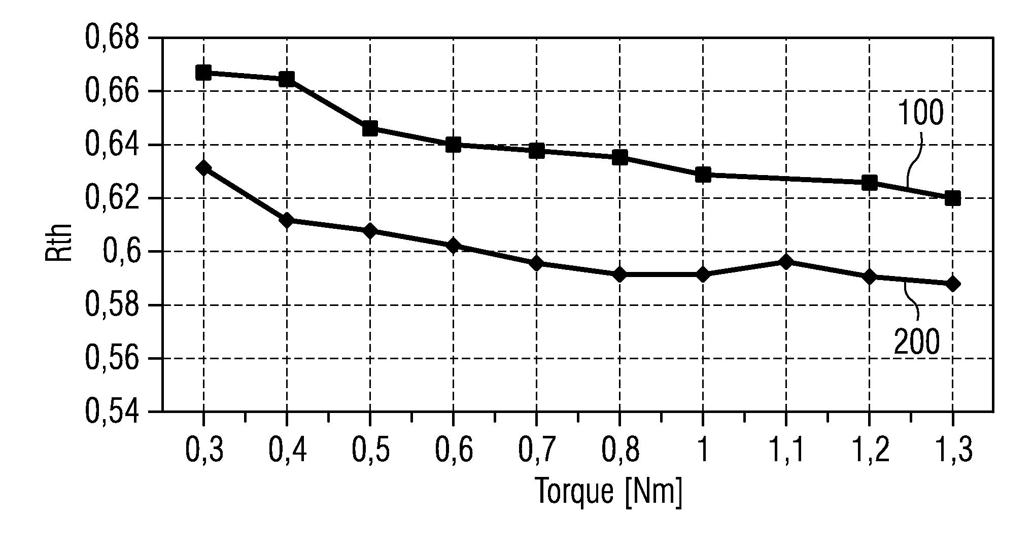
[0022]FIG. 1 shows a diagram illustrating the thermal resistance Rth of two thermally conductive pastes and semiconductor housings 100, 200 as a function of the torque exerted by means of a screw. By means of an increase in torque [Nm] in both cases the layer thicknesses of a thermally conductive paste can be reduced, which in turn leads to a reduction of the thermal resistance of the thermally conductive paste and thus to a better dissipation of the heat from the semiconductor component to the heat sink. Owing to the possibility of adjusting the layer thicknesses of the thermally conductive layer by means of the torque, the layer thicknesses and thus the heat dissipation can therefore likewise be adjusted very well.

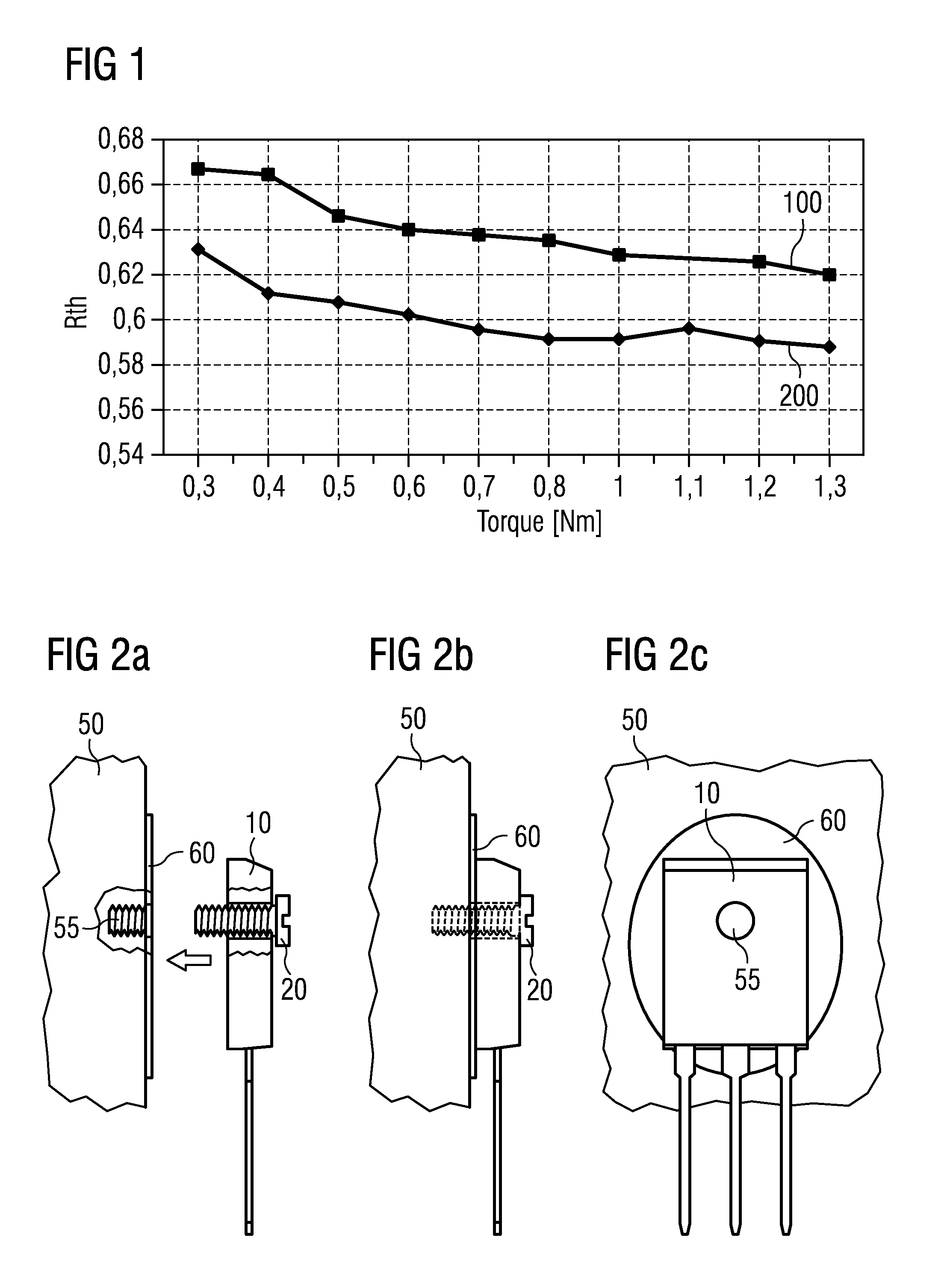
[0023]FIG. 2a shows a semiconductor housing 10 with a fixing mechanism (or device or apparatus or other means) 20. The fixing mechanism can be a screw, as shown here, or some other suitable fixing mechanism that fulfills the same function as a screw. FIG. 2a furthermore ...


PUM


Abstract

A semiconductor housing includes a fixing mechanism and at least one side having structurings. A method for producing a semiconductor device is provided in which a thermally conductive paste is applied on the at least one side of the semiconductor housing and / or of a heat sink. The semiconductor housing is fixed to the heat sink by means of the fixing mechanism. A pressure is exerted on the thermally conductive paste by means of the fixing mechanism and the thermally conductive paste is diverted by means of diversion channels depending on the pressure exerted.

Description

[0001]This application claims priority to German Patent Application 10 2012 018 943.5, which was filed Sep. 25, 2012 and is incorporated herein by reference.TECHNICAL FIELD[0002]The present invention relates to a semiconductor housing with rear-side structuring.BACKGROUND[0003]In many areas of electronics, sensor technology and microsystems engineering, the production requirements give rise to a constraint for increasing miniaturization and for increasing productivity by joining together subsystems in more highly integrated structures. The trend toward ever more highly integrated and more compact designs leads, for structural reasons, to the individual components being heated ever increasingly per unit area on account of the ever increasing performance and the power thus generally consumed. In order to ensure an effective dissipation of heat from the components particularly in the semiconductor power field, components are linked to heat sinks, for example. The dissipation of heat is...

Claims


Application Information

Patent Timeline
Patent Type & Authority Applications(United States)
IPC IPC(8): H01L23/40H01L21/50
CPCH01L21/50H01L23/4006H01L23/49562H01L2924/0002
Inventor OTREMBA, RALFHOEGLAUER, JOSEFSCHLOEGEL, XAVERSCHREDL, JUERGEN
Owner INFINEON TECH AG
Why Eureka
Try Eureka