Multi-layered board and semiconductor package

a multi-layer board and semiconductor technology, applied in the direction of solid-state devices, basic electric elements, electrical apparatus construction details, etc., can solve the problem that the heat generated by the semiconductor devices is likely to be confined in the semiconductor package, and achieve the effect of improving the heat dissipation performance of the semiconductor packag

Inactive Publication Date: 2014-03-27
FUJIFILM CORP
View PDF4 Cites 40 Cited by
  • Summary
  • Abstract
  • Description
  • Claims
  • Application Information

AI Technical Summary

Benefits of technology

[0008]According to the present invention, it is possible to improve heat dissipation performance of a semiconductor package manufactured using an anisotropically-conductive member.

Problems solved by technology

Thermal conductivity of an insulating base constituting the anisotropically-conductive member is low, and particularly, in a semiconductor package having semiconductor devices disposed on both surfaces of the anisotropically-conductive member such as a three-dimensional mounting type, heat generated from the semiconductor devices is likely to be confined in the semiconductor package.

Method used


Image

  • Multi-layered board and semiconductor package
  • Multi-layered board and semiconductor package
  • Multi-layered board and semiconductor package

Examples


first embodiment

Multi-Layered Board

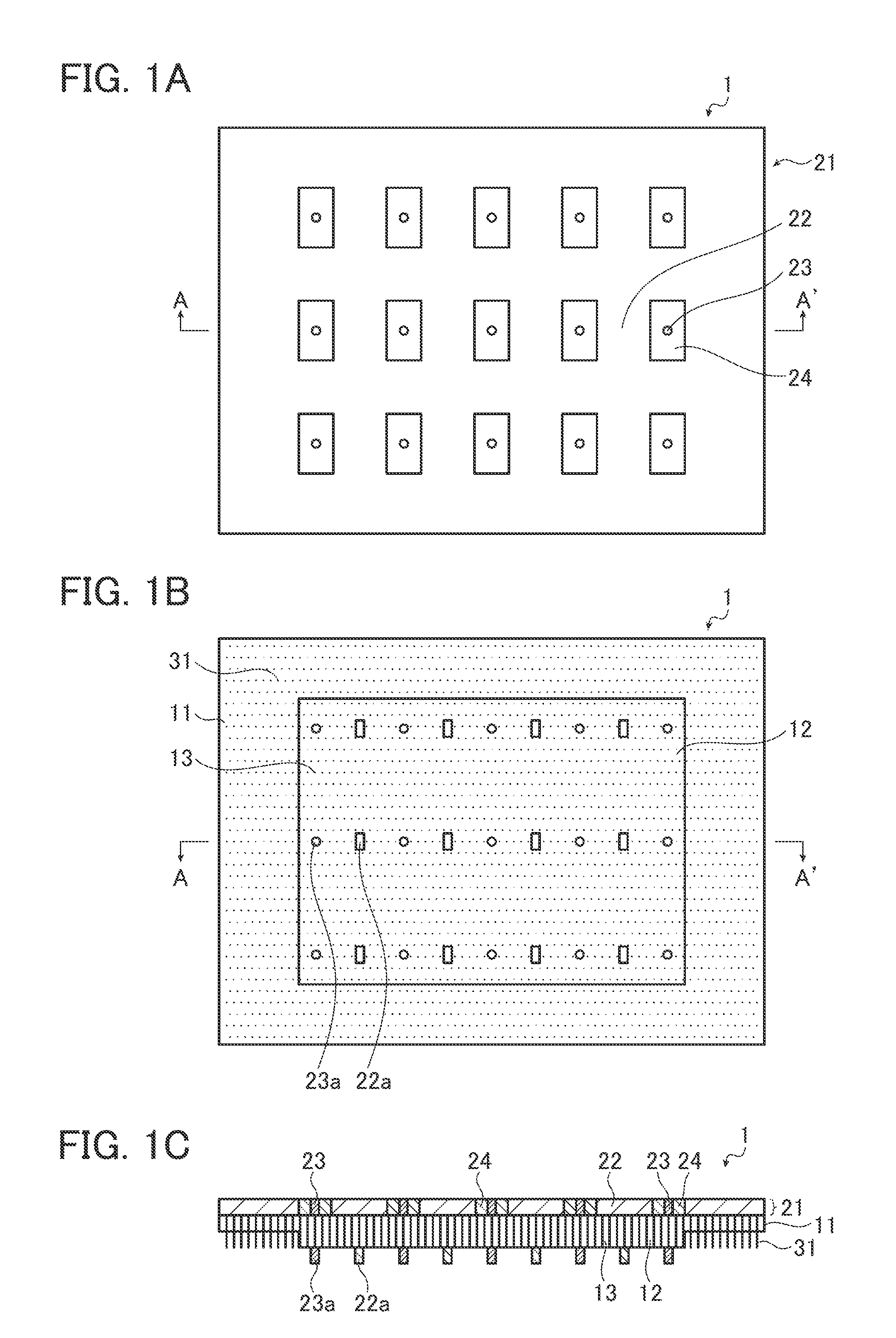
[0028]FIG. 1A is a plan view schematically illustrating a multi-layered board according to a first embodiment, FIG. 1B is a bottom view thereof, and FIG. 1C is a cross-sectional view taken along line A-A′ of FIG. 1A and line A-A′ of FIG. 1B.

[0029]The multi-layered board 1 according to the first embodiment is a multi-layered board having a layer formed of an anisotropically-conductive member 11 and a heat conducting layer 21 disposed on one surface of the anisotropically-conductive member 11. Heat dissipating portions 31 is are provided integrally in part of the anisotropically-conductive member 11.

Anisotropically-Conductive Member

[0030]The anisotropically-conductive member 11 has an insulating base 12 and plural conduction passages 13 formed of a conductive material. The conduction passages 13 are provided to extend through the insulating base 12 in the thickness direction in a state where the conduction passages are insulated from each other. The conduction passa...

second embodiment

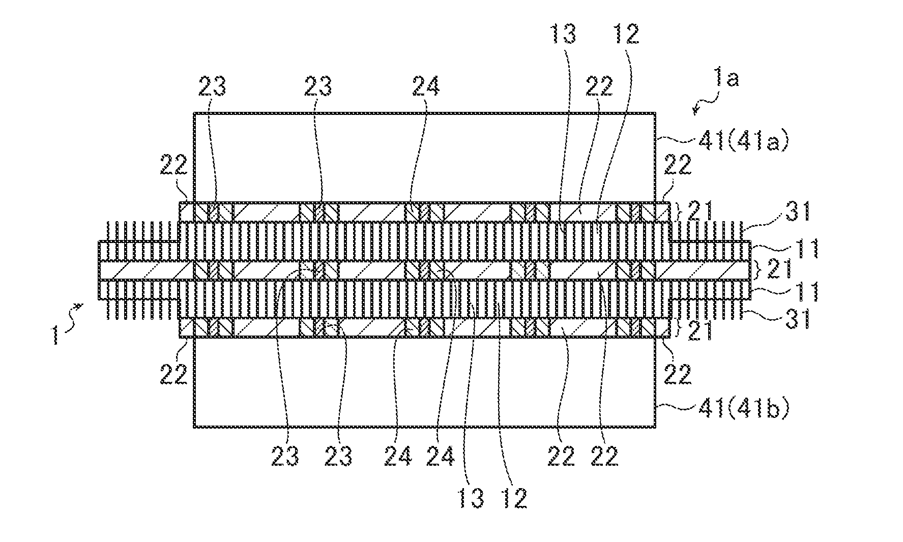
[0087]FIG. 3A is a plan view schematically illustrating a semiconductor package according to a second embodiment in which a semiconductor device is omitted and FIG. 3B is a cross-sectional view taken along line B-B′ of FIG. 3A. In the second embodiment, the same constituents as in the first embodiment are referenced by the same reference signs and description thereof will not be repeated (the same applies hereinafter).

[0088]In the second embodiment, a heat conducting layer 21 is formed on both sides of an anisotropically-conductive member 11. Each of the heat conducting layers 21 on both surfaces is also formed outside semiconductor devices 41 and has a shape in which it is connective as a whole.

[0089]However, unlike the first embodiment, on one surface of a multi-layered board 1, the heat conducting layer 21 is not formed in the outermost part and the anisotropically-conductive member 11 is exposed. Heat dissipating portions 31 are formed in the exposed portion of the anisotropical...

third embodiment

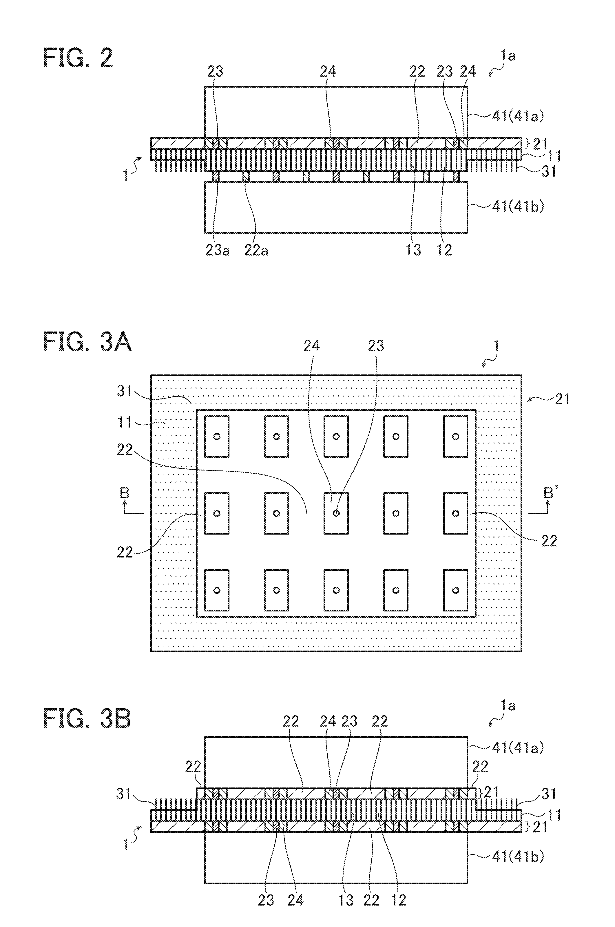
[0091]FIG. 4 is a diagram schematically illustrating a semiconductor package according to a third embodiment. In the third embodiment, heat conducting portions 22 are embedded in an anisotropically-conductive member 11.

[0092]In the heat conducting layer 21 of the first or second embodiment, miniaturization and thermal conductivity have a trade-off relationship. That is, when the heat conducting layer 21 disposed on the surface of the anisotropically-conductive member 11 increases in thickness, the thickness of the heat conducting portions 22 also increases. Accordingly, the heat conductivity is improved but the thickness of the interconnecting portions 23 also increases, which runs contrary to the miniaturization. On the other hand, when the heat conducting layer 21 decreases in thickness to miniaturize the interconnecting portions 23, the thickness of the heat conducting portions 22 also decreases and thus the thermal conductivity is relatively lowered.

[0093]However, as in the thir...


PUM


Abstract

The invention provides a multi-layered board and a semiconductor package including the multi-layered board with improved heat dissipation performance of the semiconductor package. A multi-layered board includes an anisotropically-conductive member that includes an insulating base which is an anodized film of an aluminum substrate and in which through-holes are formed in a thickness direction and a plurality of conduction passages which are formed of a conductive material filled in the through-holes and which extend through the insulating base in the thickness direction with the conduction passages insulated from each other, a heat conducting layer that includes heat conducting portions and is disposed on at least one surface of the anisotropically-conductive member, and heat dissipating portions formed of the conductive material and protruding from the insulating base.

Description

BACKGROUND OF THE INVENTION[0001]The present invention relates to a multi-layered board including an anisotropically-conductive member and a semiconductor package using the multi-layered board.[0002]A three-dimensional mounting technique is known for being a trend of semiconductor mounting techniques. By employing this technique, even a semiconductor device manufactured using design rules of former generations can exhibit the same performance as the newest semiconductor devices and a data transmission rate between different types of semiconductor devices can be raised.[0003]As an application example of the three-dimensional mounting technique, a configuration in which an IC chip (semiconductor device) and an anisotropically-conductive film (anisotropically-conductive member) are alternately superimposed is disclosed in FIG. 6 of JP 2009-164095 A.SUMMARY OF THE INVENTION[0004]Thermal conductivity of an insulating base constituting the anisotropically-conductive member is low, and par...

Claims


Application Information

Patent Timeline
Patent Type & Authority Applications(United States)
IPC IPC(8): H05K1/02
CPCH05K1/0204H01L2224/16225H01L23/142H01L23/3677H01L23/49827H01L2225/06589H01L2924/13055H01L2924/1461H01L23/3733H01L2924/1305H01L2924/12044H01L2924/00H01L23/13H01L23/34H01L23/36H01L23/42
Inventor YAMASHITA, KOSUKE
Owner FUJIFILM CORP
Why Eureka
Try Eureka