Check patentability & draft patents in minutes with Patsnap Eureka AI!

Optical communication module and assembling method thereof

a technology of optical communication module and optical communication module, which is applied in the direction of optical elements, electromagnetic transceivers, instruments, etc., can solve the problems of erroneous signal transmission and conversion, and loss of output energy, so as to enhance the three-dimensional stability of optical communication module and increase the overall coupling performance of optical communication module

Active Publication Date: 2014-03-27
DELTA ELECTRONICS INC
View PDF24 Cites 4 Cited by
  • Summary
  • Abstract
  • Description
  • Claims
  • Application Information

AI Technical Summary

Benefits of technology

The present invention provides an optical communication module and an assembling method that enhances the stability and overall coupling performance of the module. This is achieved by mechanically combining a ferrule and a lens carrier, and clamping them with a clipping element to ensure three-dimensional stability.

Problems solved by technology

If any one of the components is suffered from misalignment, the signal transmission and conversion may be erroneous.
Under this circumstance, the output signals are erroneous or the output energy is lost.
For example, if one of the components is shifted by an external force during the assembling process, the optical cable connecting mechanism 1 is readily suffered from misalignment.
Moreover, if the optical cable connecting mechanism 1 does not have precise optical alignment, the photoelectric conversion is possibly unable to convert signals.
Under this circumstance, the product yield or the product quality is impaired.

Method used


Image

  • Optical communication module and assembling method thereof
  • Optical communication module and assembling method thereof
  • Optical communication module and assembling method thereof

Examples


Embodiment Construction

[0024]The present invention will now be described more specifically with reference to the following embodiments. It is to be noted that the following descriptions of preferred embodiments of this invention are presented herein for purpose of illustration and description only. It is not intended to be exhaustive or to be limited to the precise form disclosed.

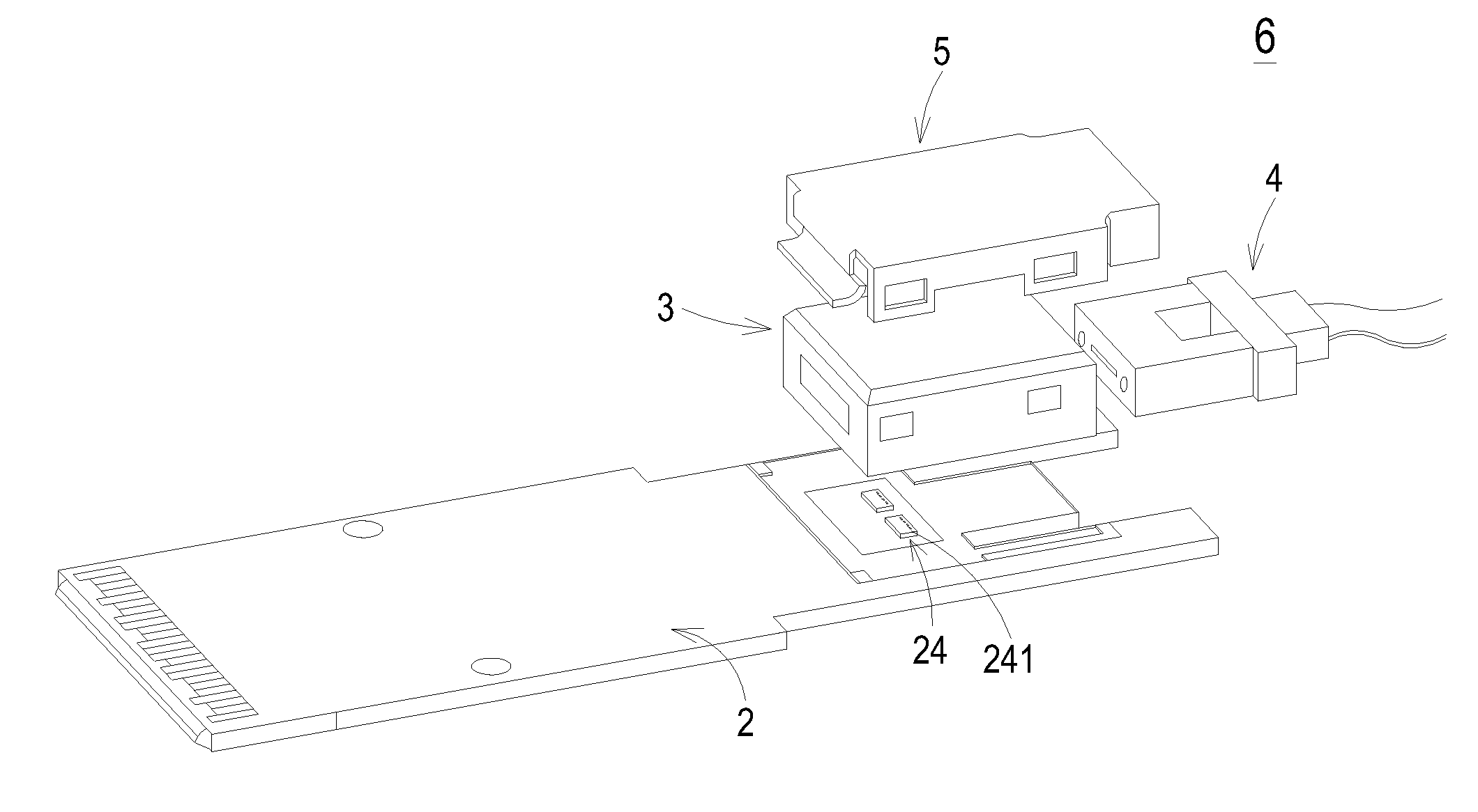
[0025]FIG. 2 is a schematic exploded view illustrating an optical communication module according to an embodiment of the present invention. As shown in FIG. 2, the optical communication module 6 comprises a substrate 2, a lens carrier 3, and a ferrule 4. Optionally, the optical communication module 6 further comprises a clipping element 5.

[0026]Moreover, at least two transmitter / receiver chips 24 (e.g. LD / PD chips) are disposed on the substrate 2. Each transmitter / receiver chip 24 comprises plural optoelectronic units 241, wherein each optoelectronic unit 241 has an alignment mark (not shown).

[0027]The lens carrier 3 comprises a ...


PUM

PropertyMeasurementUnit
optical alignmentaaaaaaaaaa
sizeaaaaaaaaaa
speedaaaaaaaaaa

Abstract

An optical communication module includes a substrate, a lens carrier, and a ferrule. The substrate includes at least two transmitter / receiver chips. The transmitter / receiver chips include plural optoelectronic units with respective alignment marks. The lens carrier includes a frame and a lens array. The lens array includes plural lens units corresponding to respective optoelectronic units of the transmitter / receiver chips of the substrate. The ferrule is coupled with the lens carrier. The alignment marks of the plural optoelectronic units are passively aligned with corresponding lens units, so that the lens carrier and the substrate are precisely aligned with each other and combined together. After the lens carrier and the substrate are combined together, the ferrule and the lens carrier are combined together, so that a precise optical communication path is constructed.

Description

FIELD OF THE INVENTION[0001]The present invention relates to an optical communication module, and more particularly to an optical communication module with a lens carrier. The present invention also relates to a method of assembling the optical communication module.BACKGROUND OF THE INVENTION[0002]With the rapid development of information technology, the demands on information communication and transmission are gradually increased, and thus the demands on the data transmission speed and the bandwidth are correspondingly increased. For transmitting numerous data in the communication network, the optical communications industries of using photoelectric conversion to transmit signals are flourishing.[0003]In the optical communications industries, optical signals are converted into electrical signals or electrical signals are converted into optical signals, and the converted optical / electrical signals are transferred through optical fibers. As known, the components in the optical transm...

Claims


Application Information

Patent Timeline
Patent Type & Authority Applications(United States)
IPC IPC(8): G02B6/36G02B6/43
CPCG02B6/43G02B6/36G02B6/4224G02B6/425G02B6/4292Y10T29/49117G02B6/32G02B6/42H04B10/40
Inventor CHEN, HSIU-PINGYOU, HONG-BINWENG, CHIA-KAI
Owner DELTA ELECTRONICS INC
Features
  • R&D
  • Intellectual Property
  • Life Sciences
  • Materials
  • Tech Scout
  • Unparalleled Data Quality
  • Higher Quality Content
  • 60% Fewer Hallucinations
Learn More