Multi-mode filter

Inactive Publication Date: 2014-04-10
MESAPLEXX
3 Cites 11 Cited by

AI-Extracted Technical Summary

Problems solved by technology

Cascading resonators in this way typically results in a significant increase in the loss in the (wanted) pass-band, due to both the insertion loss of the ...

Method used

[0042]The upper conductive layer 110 of the carrier 108 is formed with first and second trenches 136a, 136b of an electrically conductive material such as copper which presents a low impedance to radio frequency currents. The trenches 136a, 136b surround the lower faces of the first and second dielectric resonators 102a, 102b in the plane of the upper conductive layer 110, as can be seen more clearly from FIG. 4, and extending from an upper surface of the upper conductive layer 110 into the carrier 108. Each of the first and second trenches 136a, 136b has a base portion 138 which is positioned adjacent the upper groundplane 114, and is electrically coupled to the upper groundplane 114 by means of vias 140 or by directly bonding the base portion 138 of the trench 136a, 136b to the upper groundplane 114, for example using a conductive bond such as solder, or plating using an electroplating process. Thus, as can be seen most clearly in FIG. 3, the combination of the upper conductive layer 110, side walls 142 and base portions 138 of the trenches 136a, 136b and the upper groundplane 114, forms respective first and second continuous electrically conductive enclosing formations, as shown in dashed outline at 144a and 144b. These electrically conductive enclosing formations 144a, 144b are electrically grounded by virtue of the upper groundplane 114, and are electrically coupled to the electrically conductive coatings 104 of the first and second dielectric resonators 102a, 102b, and thus the first and second dielectric resonators 102a, 102b are substantially enclosed in respective first and second grounded electrically conductive enclosures made up of the coatings 104 and the respective first and second enclosing formations 144a, 144b. These grounded electrically conductive enclosures have the effect of enclosing fields (electric or magnetic) present in the dielectric resonators 102a, 102b, thus improving isolation of, and reducing leakage from, the dielectric resonators 102a, 102b, and thus lead to improved characteristics of the filter 100 in comparison to filters such as that illustrated in FIG. 2. In the example illustrated in FIG. 3 the trenches 136a, 136b take the form of open-topped channels with a generally rectangular cross-section, but it will be appreciated that the same effect can be achieved using trenches of any cross-sectional shape, for example a trench with a generally U-shaped cross-section, such that the base portion is curved, a trench having a generally V-shaped cross-section, or a trench with substantially parallel sides and a base portion having a generally V-shaped cross-section.
[0047]The carrier 208 is formed with first and second trenches 230a, 230b of an electrically conductive material such as copper which presents a low impedance to radio frequency currents. The trenches 230a, 230b surround the lower faces of the first and second dielectric resonators 202a, 202b in the plane of the upper groundplane layer 210, as can be seen more clearly from FIG. 6. The trenches 230a, 230b extend from an upper surface of the upper conductive layer 210 into the carrier 208 through the upper and lower PCB dielectric layers 218, 216 and the central connection layer 214, such that a base portion 232 of each trench 230a, 230b is positioned adjacent the lower groundplane 212. The base portion 232 of each trench 230a, 230b is electrically coupled to the lower groundplane 212 by means of a via 234 or by directly bonding the base portion 232 of the trench 230a, 230b to the lower groundplane 212, for example using a conductive bond such as solder, or plating using an electroplating process. Thus, the combination of the upper conductive layer 210, side walls 236 and base portions 232 of the trenches 230a, 230b and the lower groundplane 212, forms respective first and second electrically conductive enclosing formations, as indicated in dashed outline at 238a and 238b in FIG. 5. These electrically conductive enclosing formations 238a, 238b are electrically grounded by virtue of the lower groundplane 212, and are electrically coupled to the electrically conductive coatings 204 of the first and second dielectric resonators 202a, 202b, and thus the first and second dielectric resonators 202a, 202b are substantially enclosed in respective first and second grounded electrically conductive enclosures made up of the coatings 204 and the respective first and second enclosing formations 238a, 238b. These grounded ele...

Benefits of technology

[0007]The enclosure formed by the combination of the enclosing formation and the covering of the dielectric resonator has the effect of substantially reducing leakage from the resonator, thereby permitting an improvement in filter cha...

Abstract

The present invention relates to a multi-mode filter comprising a carrier on which is mounted a dielectric resonator having a covering of an electrically conductive material in which there is provided an aperture and a coupling structure for coupling input signals to the dielectric resonator or for extracting filtered output signals from the dielectric resonator. The carrier is provided with an enclosing formation of electrically conductive material, which enclosing formation is electrically coupled to the electrically conductive covering of the dielectric resonator, such that the covering and the enclosing formation together form an electrically conductive enclosure for the dielectric resonator. The enclosure formed from the covering of the dielectric resonator and the enclosing formation increases the isolation of the filter and reduces leakage. The filter of the present invention is particularly suitable for use in cascaded resonator filter arrangements, and in duplex/diplex filters.

Application Domain

Cross-talk/noise/interference reductionHigh frequency circuit adaptations +2

Technology Topic

Electrically conductiveConductive materials +4

Image

  • Multi-mode filter
  • Multi-mode filter
  • Multi-mode filter

Examples

  • Experimental program(1)

Example

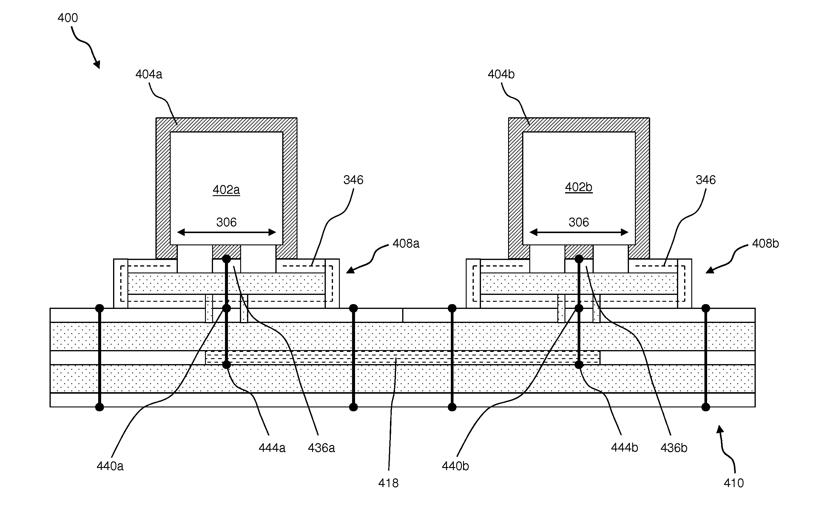
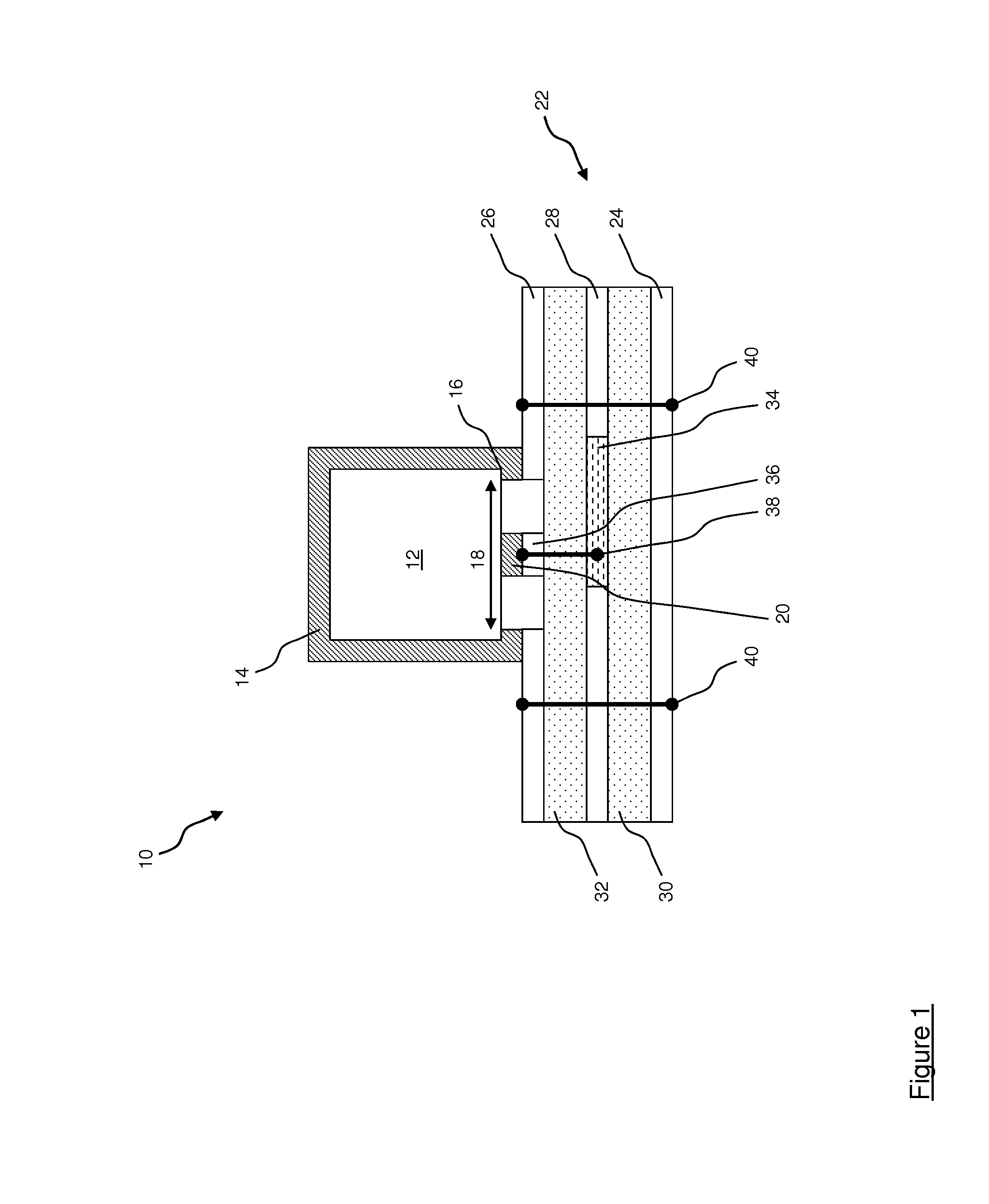
[0030]FIG. 1 is a schematic cross-sectional representation of a multi-mode dielectric filter. In the example illustrated in FIG. 1, the multi-mode filter (shown generally at 10) comprises a dielectric resonator 12, which in the example is in the form of a generally cuboidal “puck” of dielectric material such as a ceramic material having a high dielectric constant. The cuboidal puck of dielectric material 12 is provided on five of its six faces with a coating or covering 14 of an electrically conductive material such as silver or another electrically conductive metal. The coating 14 extends also partially over a sixth face 16 of the dielectric material 12, thereby defining an aperture 18 in the coating 14 on the sixth face 16. One or more coupling structures 20 are provided on the sixth face 16 of the dielectric material to permit a signal to be filtered to be input to the dielectric material 12 and/or to permit filtered output signals to be extracted from the dielectric material 12.
[0031]The dielectric resonator 12 is mounted on a carrier 22, which in the example illustrated in FIG. 1 is a printed circuit board (PCB), but which may alternatively be of another dielectric material such as ceramic or glass. The PCB has lower and upper groundplane layers 24, 26 and a central connection layer 28. Lower and upper layers 30, 32 of PCB dielectric material having a low dielectric constant are disposed between the lower groundplane layer 24 and the central connection layer 28 and between the central connection layer 28 and the upper groundplane layer 26 respectively. The upper groundplane layer 26 includes an aperture generally corresponding in shape and size to the aperture 18 in the coating 14 of the dielectric resonator 12. The central connection layer 28 includes an input or output connection track 34 which is electrically connected by means of a via 38 to a PCB connection track 36 disposed within the aperture of the upper groundplane layer 26, the PCB connection track 26 being electrically isolated from the upper groundplane layer 26. Further vias 40 electrically connect the upper and lower groundplane layers 24, 26.
[0032]With the dielectric resonator 12 positioned on the carrier 22 as illustrated in FIG. 1, the coating 14 of the dielectric resonator 12 is electrically coupled to the upper groundplane 26 of the carrier, and the coupling structure 20 of the dielectric material 12 is electrically coupled to the PCB connection track 36, which is in turn electrically coupled to the input or output connection track 34. Thus, a signal to be filtered can be input to the dielectric resonator 12 or a filtered output signal can be extracted from the dielectric resonator 12 as appropriate by means of the input or output connection track 24.
[0033]Multi-mode filters such as the one illustrated in FIG. 1 typically have a low cost structure, a low loss and a small size. This is essential in active antenna applications where many filters are required in each active antenna product. For example, a 900 MHz active antenna product typically requires 16 filters. Unless small, low-cost, low-loss filters are used, the product becomes either too heavy or too expensive to be deployed on a large scale.
[0034]Some applications require a sharp roll-off between the pass-band and the stop band(s) of a filter, which may not be realisable using a single filter, even where a multi-mode filter such as that illustrated in FIG. 1 is used. In such applications it is typical to cascade multiple resonators 12.
[0035]Such an arrangement of cascaded resonators is shown generally at 60 in FIG. 2, which is a schematic cross-sectional view of a filter arrangement which uses two cascaded resonators. In the arrangement illustrated in FIG. 2, first and second dielectric resonators 62a, 62b are mounted on a common carrier 64, in a manner similar to that described above with reference to FIG. 1. Thus, each of the dielectric resonators 62a, 62b has an apertured coating or covering 66 of an electrically conductive material such as silver or another electrically conductive metal. The first and second dielectric resonators 62a, 62b are mounted on the carrier such that their coatings electrically couple to an upper groundplane 68 of the carrier 64.
[0036]The first dielectric resonator 62a is provided with a coupling structure 70 which is electrically coupled to a PCB connection track 72 of the carrier 64 to permit a filtered output signal to be extracted from the first dielectric resonator 62a. The second dielectric resonator 62b is provided with a coupling structure 74 which is electrically coupled to a PCB connection track 76 of the carrier 64 to permit a signal to be filtered to be input to the second dielectric resonator 62b. The PCB connection tracks 72 and 76 are each connected to a common connector track 78 by vias 80, such that a signal extracted from the first dielectric resonator 62a is input to the second dielectric resonator 62b for further filtering. In this way, the required filter characteristics can be realised using the cascaded dielectric resonators 62a, 62b.
[0037]One disadvantage of the cascaded dielectric resonator arrangement illustrated in FIG. 2 is that the overall filter losses due to the insertion loss within the dielectric resonators 62a, 62b and the coupling losses in transferring energy into and out of the dielectric resonators 62a, 62b is too high for some applications, such as diplexers for use in transceivers. It can also be difficult to achieve sufficient isolation between the individual dielectric resonators 62a, 62b in a cascaded arrangement of the type illustrated in FIG. 2 for the overall filter to achieve its theoretical capabilities, particularly with regard to stop band isolation, as leakage occurs through the carrier 64 on which the cascaded dielectric resonators 62a, 62b are mounted. In the particular case of a duplex or diplex filter configuration for use in a transceiver, leakage may also occur between the transmit and receive portions of the filter.
[0038]Referring now to FIG. 3, an arrangement of cascaded dielectric resonators forming a filter is shown generally at 100. The filter 100 is made up of two generally similar dielectric resonators 102a, 102b, each being formed as a generally cuboidal puck of a dielectric material such as a ceramic having a high dielectric constant. Each of the dielectric resonators 102a, 102b has a coating or covering of an electrically conductive material such as silver or another electrically conductive metal. The coating 104 extends over all six faces of the dielectric resonators 102a, 102b, although apertures 106a, 106b are provided in the coating 104 in one face (shown as the lower face in FIG. 3) of each of the dielectric resonators 102a, 102b, to permit connections to be made to the dielectric material of the dielectric resonators 102a, 102b.
[0039]The first and second dielectric resonators 102a, 102b are mounted on a common carrier 108, which may be, for example, a printed circuit board (PCB), but which may alternatively be of another dielectric material such as ceramic or glass. The carrier 108 has an upper conductive layer 110 of a conductive material such as copper, lower and upper groundplane layers 112, 114 and a central connection layer 116. Lower and upper layers 118, 120 of PCB dielectric material having a low dielectric constant are disposed between the lower groundplane layer 112 and the central connection layer 116 and between the central connection layer 116 and the upper groundplane layer 114 respectively. A further layer 122 of dielectric material such as PCB material, ceramic or glass is disposed between the upper groundplane layer 114 and the upper conductive layer 110.
[0040]The upper conductive layer 110 is provided with apertures 111a, 111b which correspond generally in shape and size to the apertures 106a, 106b of the dielectric resonators 102a, 102b. It will be appreciated that the apertures 111a, 111b in the upper conductive layer 110 need not correspond exactly to the apertures 106a, 106b of the dielectric resonators 102a, 102b. For example, the apertures 106a, 106b of the dielectric resonators 102a, 102b may be slightly larger than the apertures 111a, 111b in the upper conductive layer 326. The lower faces of the first and second dielectric resonators 102a, 102b are mounted on the upper conductive layer 110, with the apertures 106a, 106b in the coatings 104 of the dielectric resonators 102a, 102b aligned with the apertures 111a, 111b in the upper conductive layer 110, such that that portion of the electrically conductive coatings 104 which surrounds each of the apertures 106a, 106b electrically couples the coatings 104 of the dielectric resonators 102a, 102b to the upper conductive layer 110 of the carrier 108.
[0041]The first dielectric resonator 102a is provided with one or more coupling structures 124 which are electrically coupled to one or more corresponding PCB connection tracks 126 provided within the aperture 111a of the upper conductive layer 110 of the carrier 108, to permit a signal to be filtered to be input to the first dielectric resonator 102a, and/or to permit a filtered output signal to be extracted from the first dielectric resonator 102a. Similarly, the second dielectric resonator 102b is provided with one or more coupling structures 128 which are electrically coupled to PCB connection tracks 130 provided within the aperture 111b of the upper conductive layer 110 of the carrier 108, to permit a signal to be filtered to be input to the second dielectric resonator 102b, and/or to permit a filtered output signal to be extracted from the second dielectric resonator 102b. The PCB connection tracks 126 and 130 are each connected to a common connector track 132 by vias 134, such that a signal extracted from the first dielectric resonator 102a is input to the second dielectric resonator 102b for further filtering.
[0042]The upper conductive layer 110 of the carrier 108 is formed with first and second trenches 136a, 136b of an electrically conductive material such as copper which presents a low impedance to radio frequency currents. The trenches 136a, 136b surround the lower faces of the first and second dielectric resonators 102a, 102b in the plane of the upper conductive layer 110, as can be seen more clearly from FIG. 4, and extending from an upper surface of the upper conductive layer 110 into the carrier 108. Each of the first and second trenches 136a, 136b has a base portion 138 which is positioned adjacent the upper groundplane 114, and is electrically coupled to the upper groundplane 114 by means of vias 140 or by directly bonding the base portion 138 of the trench 136a, 136b to the upper groundplane 114, for example using a conductive bond such as solder, or plating using an electroplating process. Thus, as can be seen most clearly in FIG. 3, the combination of the upper conductive layer 110, side walls 142 and base portions 138 of the trenches 136a, 136b and the upper groundplane 114, forms respective first and second continuous electrically conductive enclosing formations, as shown in dashed outline at 144a and 144b. These electrically conductive enclosing formations 144a, 144b are electrically grounded by virtue of the upper groundplane 114, and are electrically coupled to the electrically conductive coatings 104 of the first and second dielectric resonators 102a, 102b, and thus the first and second dielectric resonators 102a, 102b are substantially enclosed in respective first and second grounded electrically conductive enclosures made up of the coatings 104 and the respective first and second enclosing formations 144a, 144b. These grounded electrically conductive enclosures have the effect of enclosing fields (electric or magnetic) present in the dielectric resonators 102a, 102b, thus improving isolation of, and reducing leakage from, the dielectric resonators 102a, 102b, and thus lead to improved characteristics of the filter 100 in comparison to filters such as that illustrated in FIG. 2. In the example illustrated in FIG. 3 the trenches 136a, 136b take the form of open-topped channels with a generally rectangular cross-section, but it will be appreciated that the same effect can be achieved using trenches of any cross-sectional shape, for example a trench with a generally U-shaped cross-section, such that the base portion is curved, a trench having a generally V-shaped cross-section, or a trench with substantially parallel sides and a base portion having a generally V-shaped cross-section.
[0043]FIG. 5 is a schematic cross-sectional view of an alternative arrangement of cascaded dielectric resonators forming a filter 200. As in the embodiment illustrated in FIG. 3, the filter 200 is made up of two generally similar dielectric resonators 202a, 202b, each being formed as a generally cuboidal puck of a dielectric material such as a ceramic having a high dielectric constant. Each of the dielectric resonators 202a, 202b has a coating or covering of an electrically conductive material such as silver or another electrically conductive metal. The coating 204 extends over all six faces of the dielectric resonators 202a, 202b, although apertures 206a, 206b are provided in the coating 204 in one face (shown as the lower face in FIG. 5) of each of the dielectric resonators 202a, 202b, to permit connections to be made to the dielectric material of the dielectric resonators 202a, 202b.
[0044]The first and second dielectric resonators 202a, 202b are mounted on a common carrier 208, which may be, for example, a printed circuit board (PCB), but which may alternatively be of another dielectric material such as ceramic or glass. The carrier has an upper conductive layer 210 of a conductive material such as copper, a lower groundplane layer 212 and a central connection layer 214. Lower and upper layers 216, 218 of dielectric material such as PCB material, ceramic or glass are disposed between the lower groundplane layer 212 and the central connection layer 214 and between the central connection layer 214 and the upper conductive layer 210 respectively.
[0045]The upper groundplane layer 210 is provided with apertures 211a, 211b which generally correspond in shape and size to the apertures 206a, 206b of the dielectric resonators 202a, 202b. It will be appreciated that the apertures 211a, 211b in the upper groundplane layer 210 need not correspond exactly to the apertures 206a, 206b of the dielectric resonators 202a, 202b. For example, the apertures 206a, 206b of the dielectric resonators 202a, 202b may be slightly larger than the apertures 211a, 211b in the upper groundplane layer 210. The lower faces of the first and second dielectric resonators 202a, 202b are mounted on the upper conductive layer 210, with the apertures 206a, 206b of the first and second dielectric resonators 202a, 202b aligned with the apertures 211a, 211b of the upper groundplane 210 of the carrier 208, such that that portion of the electrically conductive coatings 204 which surrounds each of the apertures 206a, 206b electrically couples the coating 204 of the dielectric resonators 202a, 202b to the upper conductive layer 210 of the carrier 208.
[0046]The first dielectric resonator 202a is provided with one or more coupling structures 220 which are electrically coupled to one or more corresponding PCB connection tracks 222 disposed within the aperture 211a of the upper groundplane layer 210 of the carrier 208 to permit a signal to be filtered to be input to the first dielectric resonator 202a, and/or to permit a filtered output signal to be extracted from the first dielectric resonator 202a. Similarly, the second dielectric resonator 202b is provided with one or more coupling structures 224 which are electrically coupled to a PCB connection track 226 disposed within the aperture 211b of the upper groundplane 210 of the carrier 208 to permit a signal to be filtered to be input to the second dielectric resonator 202b and/or to permit a filtered output signal to be extracted from the second dielectric resonator 202b. The PCB connection tracks 222 and 226 are each connected to a common connector track 228 by vias 230, such that a signal extracted from the first dielectric resonator 202a is input to the second dielectric resonator 202b for further filtering.
[0047]The carrier 208 is formed with first and second trenches 230a, 230b of an electrically conductive material such as copper which presents a low impedance to radio frequency currents. The trenches 230a, 230b surround the lower faces of the first and second dielectric resonators 202a, 202b in the plane of the upper groundplane layer 210, as can be seen more clearly from FIG. 6. The trenches 230a, 230b extend from an upper surface of the upper conductive layer 210 into the carrier 208 through the upper and lower PCB dielectric layers 218, 216 and the central connection layer 214, such that a base portion 232 of each trench 230a, 230b is positioned adjacent the lower groundplane 212. The base portion 232 of each trench 230a, 230b is electrically coupled to the lower groundplane 212 by means of a via 234 or by directly bonding the base portion 232 of the trench 230a, 230b to the lower groundplane 212, for example using a conductive bond such as solder, or plating using an electroplating process. Thus, the combination of the upper conductive layer 210, side walls 236 and base portions 232 of the trenches 230a, 230b and the lower groundplane 212, forms respective first and second electrically conductive enclosing formations, as indicated in dashed outline at 238a and 238b in FIG. 5. These electrically conductive enclosing formations 238a, 238b are electrically grounded by virtue of the lower groundplane 212, and are electrically coupled to the electrically conductive coatings 204 of the first and second dielectric resonators 202a, 202b, and thus the first and second dielectric resonators 202a, 202b are substantially enclosed in respective first and second grounded electrically conductive enclosures made up of the coatings 204 and the respective first and second enclosing formations 238a, 238b. These grounded electrically conductive enclosures have the effect of enclosing fields (electric or magnetic) present in the dielectric resonators 202a, 202b, thus improving isolation of, and reducing leakage from, the dielectric resonators 202a, 202b, and thus lead to improved characteristics of the filter 200 in comparison to filters such as that illustrated in FIG. 2. It will be noted that, in the embodiment illustrated in FIGS. 5 and 6, the common connector track 228 extends through the side walls 236 of the trenches 230a, 230b. Thus, a gap exists in each of the enclosures enclosing the dielectric resonators 202a, 202b. Nevertheless, the combination of the enclosing formations 238a, 238b and the coverings 204 to form the enclosures enclosing the dielectric resonators 202a, 202b provides improved performance compared to the filter arrangement of FIG. 2. In the example illustrated in FIG. 5 the trenches 230a, 230b take the form of open-topped channels with a generally rectangular cross-section, but it will be appreciated that the same effect can be achieved using trenches of any cross-sectional shape, for example a trench with a generally U-shaped cross-section, such that the base portion is curved, a trench having a generally V-shaped cross-section, or a trench with substantially parallel sides and a base portion having a generally V-shaped cross-section.
[0048]FIG. 7 is a schematic cross-sectional representation of an alternative dielectric resonator filter 300. In the arrangement illustrated in FIG. 7, the filter 300 uses a single dielectric resonator 302 formed as a generally cuboidal puck of a dielectric material such as a ceramic having a high dielectric constant. The dielectric resonator 302 has a coating or covering 304 of an electrically conductive material such as silver or another electrically conductive metal. The coating 304 extends over all six faces of the dielectric resonator 302, although an aperture 306 is provided in the coating 304 in one face (shown as the lower face in FIG. 7) of the dielectric resonator 302, to permit connections to be made to the dielectric material of the dielectric resonator 302.
[0049]The dielectric resonator 302 is mounted on a first carrier 308, which in turn is mounted on a second carrier 310, such that the second carrier 310 may be regarded as a “mother” carrier and the first carrier 308 may be regarded as a “daughter” carrier.
[0050]The second carrier 310 is of a dielectric material such as, for example PCB material, ceramic or glass, having lower and upper groundplane layers 312, 314, which are electrically connected by vias 316, and a central connection layer 318. Lower and upper layers 320, 322 of dielectric material such as PCB material, ceramic or glass are disposed between the lower groundplane layer 312 and the central connection layer 318 and between the central connection layer 318 and the upper groundplane layer 314 respectively.
[0051]The first carrier 308 comprises a central layer 324 of a dielectric material such as PCB substrate material, ceramic or glass. Disposed on upper and lower faces of the central layer 324 are upper and lower conductive layers 326, 328 of an electrically conductive material such as copper or another metal which presents a low impedance to radio frequency currents. The lower conductive layer 328 is disposed on and electrically coupled to the upper groundplane layer 314 of the second carrier 310. The central layer 324 of the first carrier 310 also has walls 330 of an electrically conductive material such as copper or another metal, which are electrically coupled to the upper and lower conductive layers 326, 328.
[0052]The upper conductive layer 326 is provided with an aperture 332 of a shape and size generally corresponding to the aperture 306 in the coating 304 of the dielectric resonator 302. It will be appreciated that the aperture 332 in the upper conductive layer 326 need not correspond exactly to the aperture 306 in the coating 304 of the dielectric resonator 302. For example, the aperture 306 in the coating 304 may be slightly larger than the aperture 332 in the upper conductive layer 326. The lower face of the dielectric resonator 302 is mounted on the upper conductive layer 326, with the aperture 306 of the dielectric resonator 302 aligned with the aperture 332 of the upper conductive layer 326 of the first carrier 308, such that that portion of the electrically conductive coating 304 which surrounds the aperture 306 electrically couples the coating 304 of the dielectric resonator 302 to the upper conductive layer 326 of the first carrier 308.
[0053]The dielectric resonator 302 is provided with one or more coupling structures 334 which are electrically coupled to one or more corresponding PCB connection tracks 336 disposed within the aperture 332 of the upper conductive layer 326 of the first carrier 308 to permit a signal to be filtered to be input to the dielectric resonator 302, and/or to permit a filtered output signal to be extracted from the dielectric resonator 302. The PCB connection track 336 is electrically connected to a further PCB connection track 338 provided on the lower conductive layer 328 of the first carrier 308 by a via 340. This further PCB connection track 338 is electrically coupled to a PCB connection pad 342 provided in the upper groundplane layer 314 of the second carrier 310, which PCB connection pad 342 is electrically coupled to the central connection layer 318 by means of a via 344, to permit input and output signals to be input to and extracted from the dielectric resonator 302 through the central connection layer 318.
[0054]It will be appreciated that the upper conductive layer 326, the lower conductive layer 328 and the walls 330 of the first carrier 308 together constitute a continuous electrically conductive enclosing formation, as indicated in dashed outline at 346. This electrically conductive enclosing formation 346 is electrically grounded, by virtue of the electrical connection between the lower conductive layer 328 and the upper groundplane layer 314 of the second carrier 310, and is electrically coupled to the electrically conductive coating 304 of the dielectric resonators 302, and thus the dielectric resonator 302 is substantially enclosed in a grounded electrically conductive enclosure made up of the coating 304 and the enclosing formation 346. This grounded electrically conductive enclosure has the effect of enclosing fields (electric or magnetic) present in the dielectric resonator 302, thus improving isolation of, and reducing leakage from, the dielectric resonator 302, and thus leads to improved characteristics of the filter 300 in comparison to filters such as that illustrated in FIG. 1.
[0055]FIG. 8 is a schematic cross-sectional representation of a filter arrangement 400 made up of two cascaded filters of the type described above with reference to FIG. 7.
[0056]The filter arrangement illustrated in FIG. 8 uses first and second dielectric resonators 402a, 402b of the type described above, and so like reference numerals have been used in FIG. 8 to refer to like elements. The first and second dielectric resonators 402a, 402b are mounted on respective first (“daughter”) carriers 408a, 408b, which are in turn mounted on a second carrier 410. The dielectric resonators 402a, 402b and the first carriers 408a, 408b are of the type described above, and so will not be described again in detail here.
[0057]The second carrier 410 is similar in structure and construction to the second carrier 310 described above, and so will not be described again in detail here. However, the second carrier 410 differs from the second carrier 310 described above in that that the central connection layer 418 is used to connect an output of the first dielectric resonator 402a to an input of the second dielectric resonator by means of vias 440a, 444a and 440b, 440b which connect PCB connection tracks 436a, 436b to each other, thereby permitting transfer of signals between the first and second dielectric resonators 402a, 402b.
[0058]As in the single resonator filter 300 illustrated in FIG. 7, the upper conductive layer 326, the lower conductive layer 328 and the walls 330 of the first carrier 308 together constitute a continuous electrically conductive enclosing formation, as indicated in dashed outline at 346. This electrically conductive enclosing formation 346 is electrically coupled to the electrically conductive coating 304 of the dielectric resonators 302, and thus the dielectric resonator 302 is substantially enclosed in a conductive enclosure made up of the coating 304 and the enclosing formation 346. This electrically conductive enclosure has the effect of enclosing fields (electric or magnetic) present in the dielectric resonator 302, thus improving isolation of, and reducing leakage from, the dielectric resonator 302, and thus leads to improved characteristics of the filter 300 in comparison to filters such as that illustrated in FIG. 1. In the filter 400 illustrated in FIG. 8, which uses two cascaded dielectric resonators 402a, 402b, this improved isolation and reduced leakage results in improved filter characteristics over known cascaded dielectric resonator arrangements.
[0059]It will be appreciated that the filter arrangement of the present invention provide improved isolation and reduced leakage, which gives rise to improved filter characteristics and performance, particularly in the cascaded resonator filter arrangements discussed above by reference to FIGS. 3, 5 and 8. Additionally, the filter arrangement of the present invention may be employed in a duplex or diplex filter arrangement in which a transmit filter and a receive filter are mounted on a common carrier, by electrically isolating the connecting structures of the transmit and receive structures from each other. In such an arrangement the improved isolation and reduced leakage of the filter of the present invention gives rise to improved filter characteristics and performance of both the transmit filter and the receive filter.

PUM

no PUM

Description & Claims & Application Information

We can also present the details of the Description, Claims and Application information to help users get a comprehensive understanding of the technical details of the patent, such as background art, summary of invention, brief description of drawings, description of embodiments, and other original content. On the other hand, users can also determine the specific scope of protection of the technology through the list of claims; as well as understand the changes in the life cycle of the technology with the presentation of the patent timeline. Login to view more.

Similar technology patents

Semiconductor device and manufacturing method thereof

InactiveUS20100006976A1reduce deterioration of dielectric constantreduce leakage
Owner:NEC CORP

Backlight Unit and Liquid Crystal Display Including the Same

ActiveUS20120050149A1improve luminancereduce leakage
Owner:SAMSUNG DISPLAY CO LTD

Goaf gas source comprehensive judgment and prediction method

ActiveCN106682307Areduce leakagereduce the greenhouse effect
Owner:ANHUI UNIV OF SCI & TECH +1

Classification and recommendation of technical efficacy words

  • reduce leakage

Shaft seal and turbine using the same

InactiveUS6343792B1high sealing capabilityreduce leakage
Owner:MITSUBISHI HEAVY IND LTD

Composite Passivation Process for Nitride FET

ActiveUS20090146224A1reduce leakagereduce trap
Owner:NORTHROP GRUMMAN SYST CORP

Backlight module and display device

InactiveCN105353557Areduce leakageImprove brightness and color uniformity
Owner:NANJING TECH CORP LTD

Olefin composite shaping phase-change material and preparation thereof

InactiveCN101434832Areduce leakageHigh phase change enthalpy
Owner:TIANJIN UNIV
Why Eureka
Try Eureka