Group iii nitride composite substrate and method for manufacturing the same, laminated group iii nitride composite substrate, and group iii nitride semiconductor device and method for manufacturing the same

a technology of nitride and composite substrates, which is applied in the direction of semiconductor devices, electrical equipment, basic electric elements, etc., can solve the problems of difficulty in increasing the diameter of the substrate and decreasing the thickness, and high cost of substrate manufacturing. , to achieve the effect of small thickness variation, high crystal quality and large thickness

Active Publication Date: 2014-04-17
SUMITOMO ELECTRIC IND LTD
View PDF3 Cites 21 Cited by
  • Summary
  • Abstract
  • Description
  • Claims
  • Application Information

AI Technical Summary

Benefits of technology

[0012]The present invention has been made to solve the problems above and an object of the invention is to provide a low-cost and large-diameter group III nitride composite substrate including a group III nitride film having a large thickness, a small thickness variation, and a high crystal quality, a method for manufacturing the group III nitride composite substrate, a laminated group III nitride composite substrate, and a group III nitride semiconductor device and a method for manufacturing the same.
[0021]The present invention can provide a low-cost and large-diameter group III nitride composite substrate including a group III nitride film having a large thickness, a small thickness variation, and a high crystal quality, a method for manufacturing the group III nitride composite substrate, a laminated group III nitride composite substrate, and a group III nitride semiconductor device and a method for manufacturing the same.

Problems solved by technology

The free-standing group III nitride substrate disclosed in Japanese Patent Laying-Open No. 2009-126722 involves problems that the substrate is manufactured at high cost and therefore very expensive, and that the substrate is likely to crack, resulting in difficulty in increasing the diameter of the substrate and decreasing the thickness thereof.
Regarding the GaN-thin-film-bonded substrate having the GaN thin film of 0.1 μm in thickness as disclosed in Japanese Patent Laying-Open No. 2008-010766, ion implantation is performed to form the GaN thin film, which, however, involves a problem that the ion implantation degrades the crystal quality of the GaN thin film.
An increase in thickness of the GaN thin film, however, involves a problem that the variation in depth to which ions are implanted from the main surface increases, which accordingly increases the variation in thickness of the GaN thin film in the resultant GaN-thin-film-bonded substrate.
Increase of the diameter, however, involves a problem that the variation, within the main surface, of the thickness of the GaN thin film or the GaN layer increases.
In the case where a heterogeneous substrate such as sapphire substrate whose chemical composition and thermal expansion coefficient are different from those of a group III nitride substrate is prepared and a thick group III nitride film is grown on the heterogeneous substrate, there arises problems that large warp occurs and cracks are made.

Method used


Image

  • Group iii nitride composite substrate and method for manufacturing the same, laminated group iii nitride composite substrate, and group iii nitride semiconductor device and method for manufacturing the same
  • Group iii nitride composite substrate and method for manufacturing the same, laminated group iii nitride composite substrate, and group iii nitride semiconductor device and method for manufacturing the same
  • Group iii nitride composite substrate and method for manufacturing the same, laminated group iii nitride composite substrate, and group iii nitride semiconductor device and method for manufacturing the same

Examples


first embodiment

e Composite Substrate

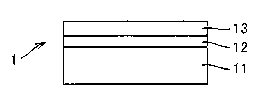
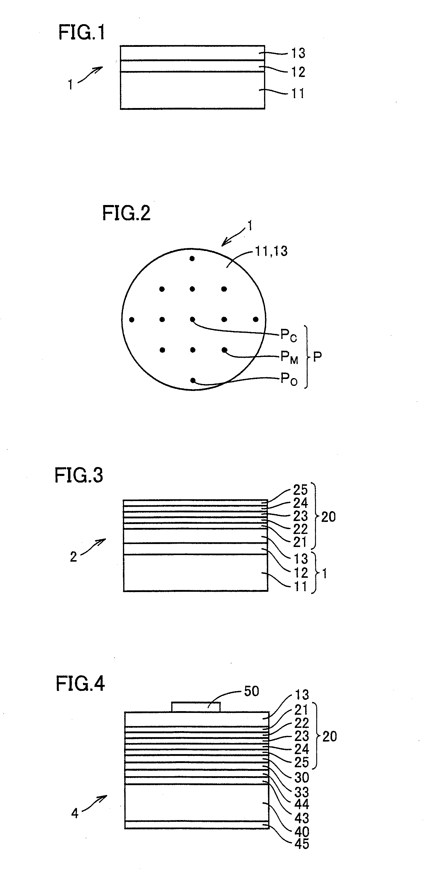
[0033]Referring to FIG. 1, a group III nitride composite substrate 1 which is an embodiment of the present invention is a group III nitride composite substrate 1 with a diameter of 75 mm or more including a support substrate 11 and a group III nitride film 13 having a thickness of 10 μm or more and 250 μm or less that are bonded to each other. The ratio st / mt of a standard deviation st of the thickness of group III nitride film 13, to a mean value mt of the thickness thereof is 0.001 or more and 0.2 or less, and the ratio so / mo of a standard deviation so of an absolute value of an off angle between a main surface of group III nitride film 13 and a plane of a predetermined plane orientation, to a mean value mo of the absolute value of the off angle thereof is 0.005 or more and 0.6 or less.

[0034]Group III nitride composite substrate 1 of the present embodiment has a diameter of 75 mm or more, group III nitride film 13 bonded onto support substrate 11 has a thickne...

second embodiment

II Nitride Composite Substrate

[0063]Referring to FIG. 3, a laminated group III nitride composite substrate 2 which is another embodiment of the present invention includes group III nitride composite substrate 1 of the first embodiment, and at least one group III nitride layer 20 disposed on group III nitride film 13 of group III nitride composite substrate 1.

[0064]In laminated group III nitride composite substrate 2 of the present embodiment, group III nitride layer 20 disposed by being grown on group III nitride film 13, which has a high crystal quality as well as a small thickness variation and a small off-angle variation, also has a high crystal quality. Therefore, semiconductor devices having excellent characteristics can be produced at a high yield.

[0065]In laminated group III nitride composite substrate 2 of the present embodiment, group III nitride layer 20 disposed on group III nitride film 13 varies depending on the type of the semiconductor device to be produced. In the ca...

third embodiment

e Semiconductor Device

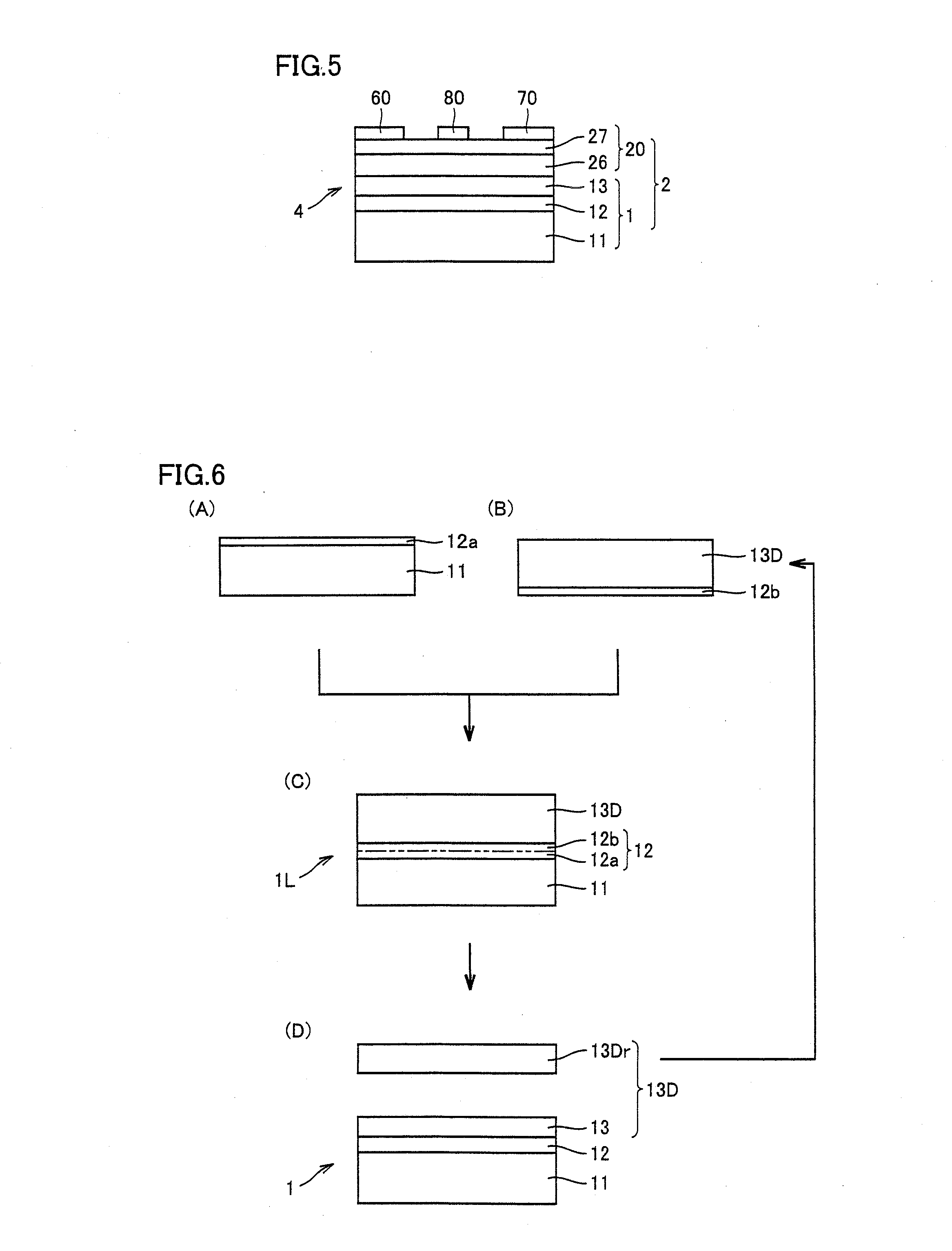
[0066]Referring to FIGS. 4 and 5, a group III nitride semiconductor device 4 which is still another embodiment of the present invention includes group III nitride film 13 in the group III nitride composite substrate of the first embodiment, and at least one group III nitride layer 20 disposed on group III nitride film 13.

[0067]Group III nitride semiconductor device 4 of the present embodiment includes group III nitride film 13 which has a high crystal quality as well as a small thickness variation and a small off-angle variation, and group III nitride layer 20 of high crystal quality disposed by being grown on group III nitride film 13, and therefore has excellent characteristics.

[0068]In group III nitride semiconductor device 4, group III nitride layer 20 varies depending on the type of group III nitride semiconductor device 4. Referring to FIG. 4, in the case where group III nitride semiconductor device 4 is a light-emitting device, group III nitride layer 20...


PUM

PropertyMeasurementUnit
thicknessaaaaaaaaaa
thicknessaaaaaaaaaa
diameteraaaaaaaaaa

Abstract

A group III nitride composite substrate includes a support substrate and a group III nitride film. A ratio st / mt of a standard deviation st of the thickness of the group III nitride film, to a mean value mt of the thickness thereof is 0.001 or more and 0.2 or less, and a ratio so / mo of a standard deviation so of an absolute value of an off angle between a main surface of the group III nitride film and a plane of a predetermined plane orientation, to a mean value mo of the absolute value of the off angle thereof is 0.005 or more and 0.6 or less. Accordingly, there is provided a low-cost and large-diameter group III nitride composite substrate including a group III nitride film having a large thickness, a small thickness variation, and a high crystal quality.

Description

BACKGROUND OF THE INVENTION[0001]1. Field of the Invention[0002]The present invention relates to a group III nitride composite substrate and a method for manufacturing the same, a laminated group III nitride composite substrate, and a group III nitride semiconductor device and a method for manufacturing the same.[0003]2. Description of the Background Art[0004]Group III nitrides such as GaN have superior semiconductor properties and are therefore used as materials suitable for semiconductor devices.[0005]For example, Japanese Patent Laying-Open No. 2009-126722 discloses a free-standing group III nitride substrate to be used as a substrate for a semiconductor device. The free-standing group III nitride substrate has a diameter of 25 mm or more and 160 mm or less and a thickness of 100 μm or more and 1000 μm or less. It discloses, as a specific example thereof, a free-standing GaN substrate having a diameter of 100 mm and a thickness of 400 μm.[0006]Japanese Patent Laying-Open No. 2008...

Claims


Application Information

Patent Timeline
Patent Type & Authority Applications(United States)
IPC IPC(8): H01L29/20
CPCH01L29/2003H01L21/2007H01L21/76254H01L29/7786H01L33/0093H01L2924/0002H01L2924/00
Inventor ISHIBASHI, KEIJIHACHIGO, AKIHIROHIROMURA, YUKIMATSUMOTO, NAOKINAKAHATA, SEIJINAKANISHI, FUMITAKEYOSHIZUMI, YUSUKEMIKAMI, HIDENORI
Owner SUMITOMO ELECTRIC IND LTD
Why Eureka
Try Eureka