Power module package

a power module and package technology, applied in the direction of semiconductor/solid-state device details, electrical equipment, semiconductor devices, etc., to achieve the effect of simplifying the process, saving process costs, and facilitating manufacturing

Inactive Publication Date: 2014-04-24
SAMSUNG ELECTRO MECHANICS CO LTD
View PDF6 Cites 7 Cited by
  • Summary
  • Abstract
  • Description
  • Claims
  • Application Information

AI Technical Summary

Benefits of technology

[0007]The present invention has been made in an effort to provide a power module packa...

Problems solved by technology

Therefore, in addition to a method for reducing a size of electronic devices, a method for installing as many device...

Method used


Image

  • Power module package
  • Power module package
  • Power module package

Examples


Embodiment Construction

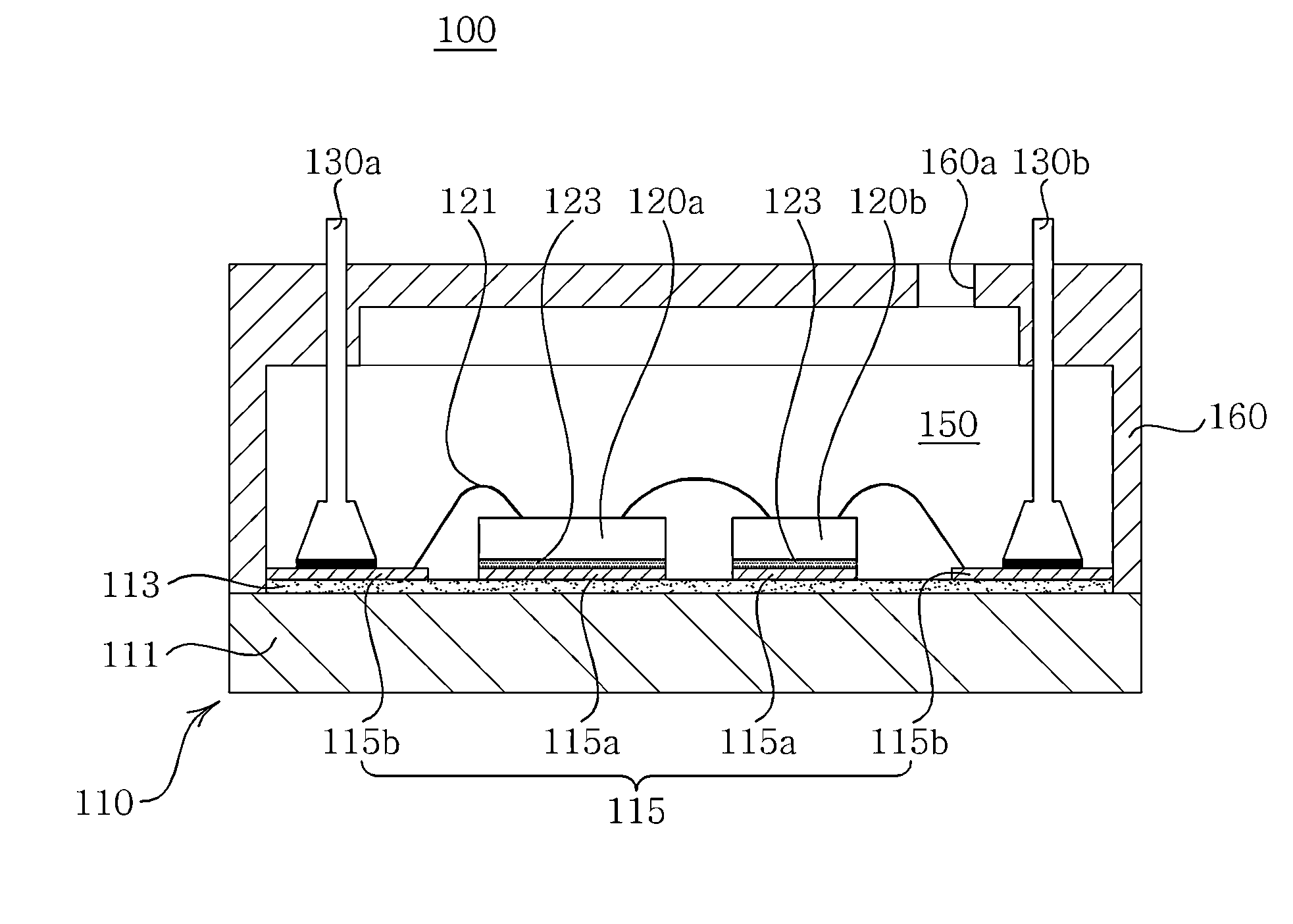
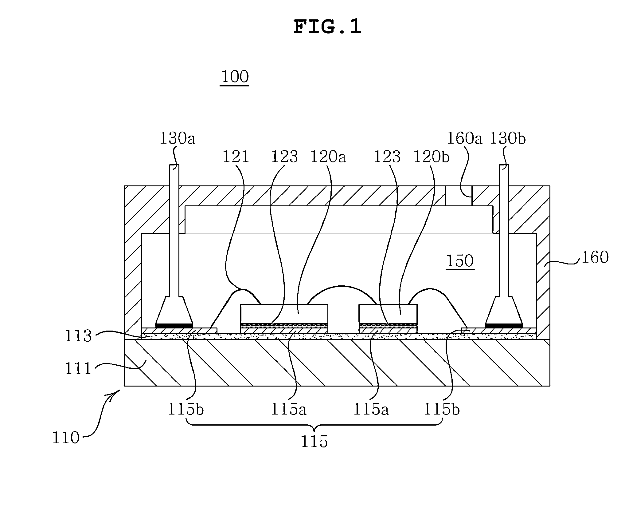
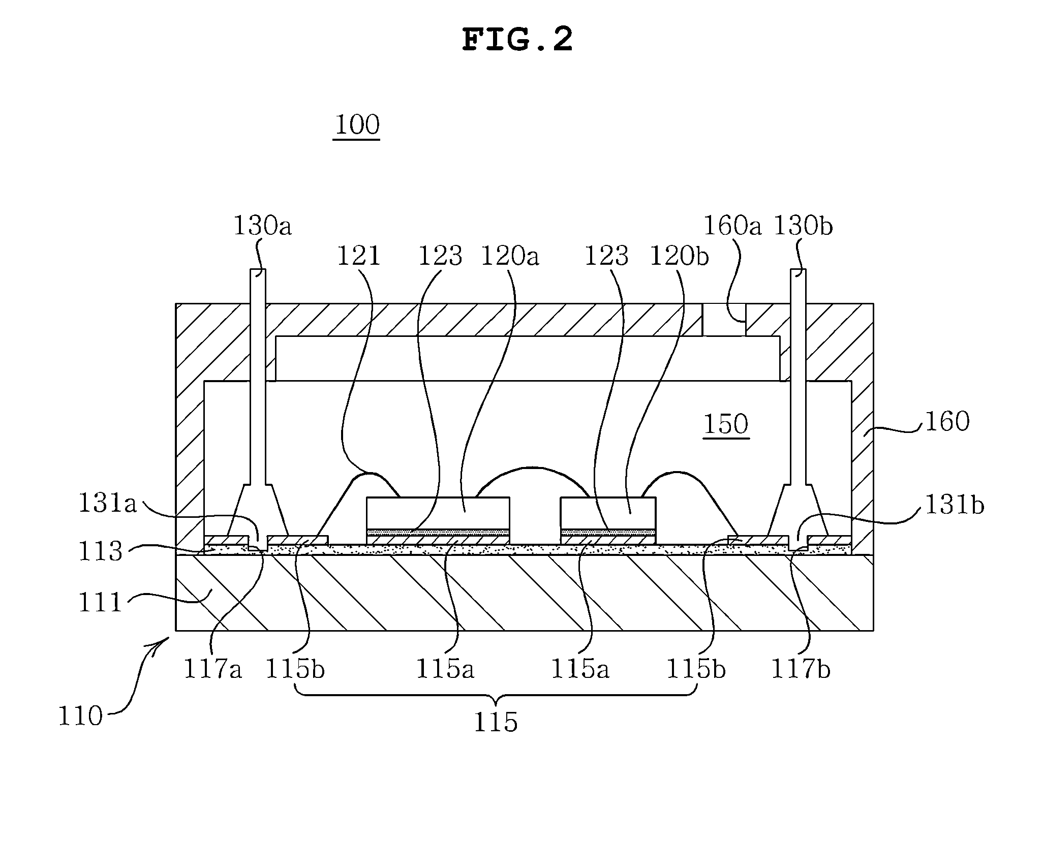
[0022]The objects, features and advantages of the present invention will be more clearly understood from the following detailed description of the preferred embodiments taken in conjunction with the accompanying drawings. Throughout the accompanying drawings, the same reference numerals are used to designate the same or similar components, and redundant descriptions thereof are omitted. Further, in the following description, the terms “first,”“second,”“one side,”“the other side” and the like are used to differentiate a certain component from other components, but the configuration of such components should not be construed to be limited by the terms. Further, in the description of the present invention, when it is determined that the detailed description of the related art would obscure the gist of the present invention, the description thereof will be omitted.

[0023]Hereinafter, preferred embodiments of the present invention will be described in detail with reference to the accompan...


PUM


Abstract

Disclosed herein is a power module package. The power module package includes a substrate having one surface formed with a circuit pattern including a chip mounting pad and an external connection pad and the other surface; a semiconductor chip mounted on the chip mounting pad; and an external connection terminal having one terminal and the other terminal, the one terminal being connected to the external connection pad and the other terminal protruding to the outside, in which the external connection pad and the external connection terminal are bonded to each other by welding.

Description

CROSS REFERENCE TO RELATED APPLICATION[0001]This application claims the benefit of Korean Patent Application No. 10-2012-0118521, filed on Oct. 24, 2012, entitled “Power Module Package” which is hereby incorporated by reference in its entirety into this application.BACKGROUND OF THE INVENTION[0002]1. Technical Field[0003]The present invention relates to a power module package.[0004]2. Description of the Related Art[0005]With the recent development of electronic industries for power, a demand for small, high-density electronic products has increased. Therefore, in addition to a method for reducing a size of electronic devices, a method for installing as many devices and conducting wires as possible within a defined space becomes an important problem in designing a power module package.[0006]Meanwhile, a structure of the power module package according to the prior art is disclosed in U.S. Pat. No. 5,920,119.SUMMARY OF THE INVENTION[0007]The present invention has been made in an effort...

Claims


Application Information

Patent Timeline
IPC IPC(8): H01L23/00
CPCH01L24/67H01L2924/13055H01L2224/32225H01L2224/48091H01L2224/48137H01L2224/48227H01L2224/73265H01L23/049H01L25/072H01L24/45H01L24/48H01L2224/45124H01L2224/45144H01L2224/45147H01L24/29H01L24/32H01L24/73H01L2224/2919H01L2924/0781H01L2224/29101H01L23/3735H01L23/42H01L23/49811H01L21/4853H01L2924/13034H01L2924/1305H01L2924/13091H01L2924/12042H01L2224/49109H01L2924/16151H01L24/49H01L2924/00H01L2924/00014H01L2924/00012H01L2924/014H01L2924/0665
Inventor YOO, DO JAEYANG, SI JOONG
Owner SAMSUNG ELECTRO MECHANICS CO LTD
Why Eureka
Try Eureka