Fabrication method for microlens array substrate

Active Publication Date: 2014-05-01
SEIKO EPSON CORP
View PDF5 Cites 16 Cited by
  • Summary
  • Abstract
  • Description
  • Claims
  • Application Information

AI Technical Summary

Benefits of technology

[0021]According to this method, the substrate can, in the step of forming the optical path length adjusting layer, be pr

Problems solved by technology

However, the inventors of this invention discovered that the annealing in this method causes the substrate to warp, causing problems in the subsequent steps of forming films and the like.
A large warp in the substrate makes it difficult to position the element substrate and the opposing substrate when affixing the substrates to each other, making it generally difficult to affix the element substrate and the opposing substrate to each other.
A large warp in the substr

Method used


Image

  • Fabrication method for microlens array substrate
  • Fabrication method for microlens array substrate
  • Fabrication method for microlens array substrate

Examples


Embodiment Construction

[0034]Hereinafter, an embodiment of the invention will be described in detail with reference to the drawings. It should be noted that in the appended drawings, the scale of the various constituent elements has been changed as appropriate to make the constituent elements more visibly recognizable.

Microlens Array Substrate

[0035]First, a microlens array substrate that can be fabricated through the microlens array substrate fabrication method according to the invention will be described with reference to FIGS. 1 and 2.

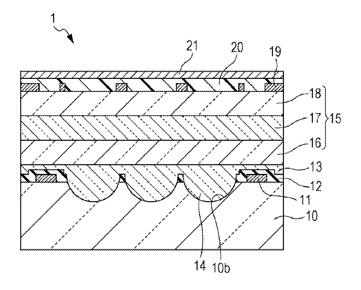
[0036]FIG. 1 is a cross-sectional view of a microlens array substrate 1 according to an embodiment of the invention.

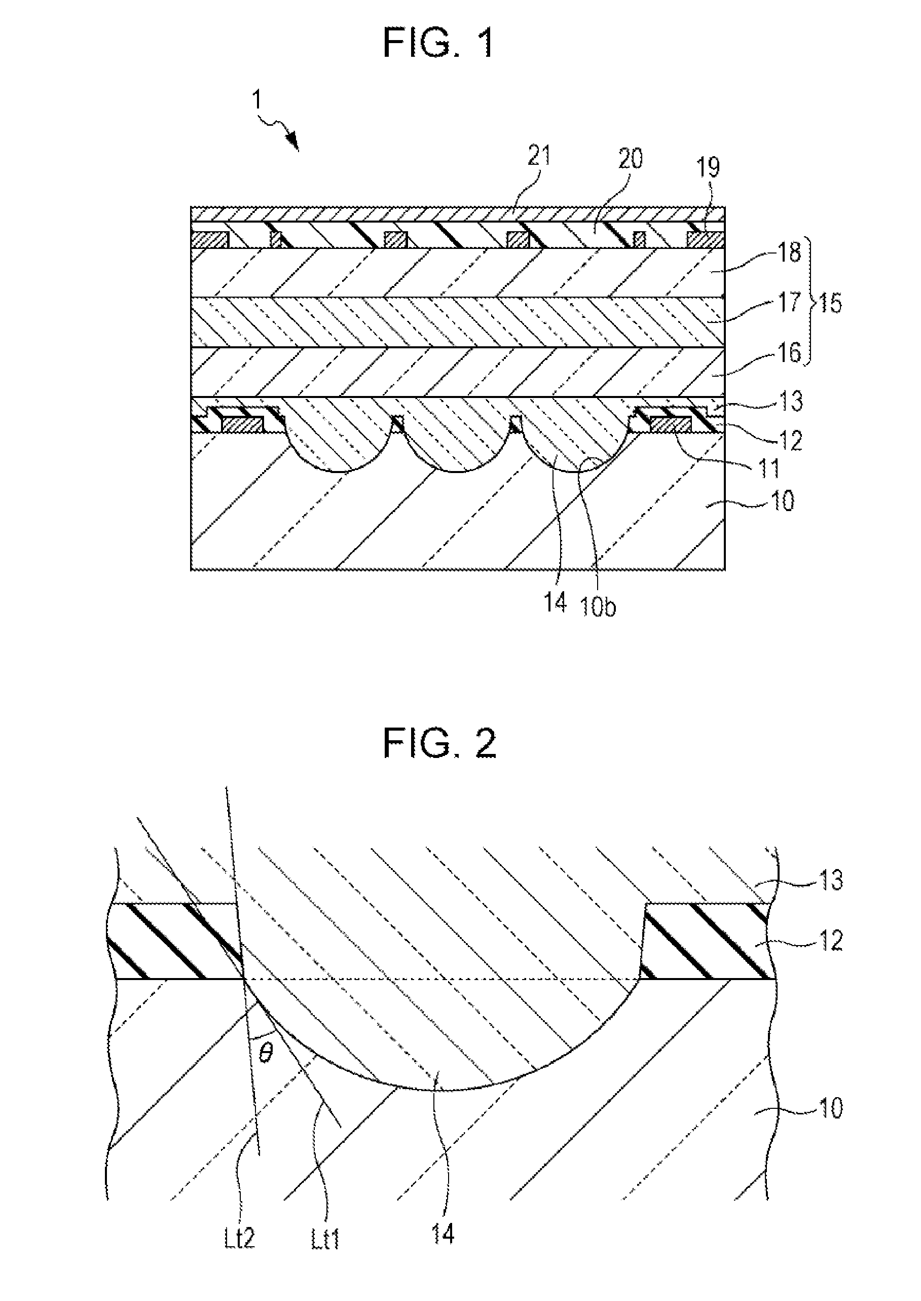
[0037]FIG. 2 is a cross-sectional partial enlargement of the microlens array substrate 1 (that is, an enlarged cross-sectional view of a microlens 14).

[0038]As shown in FIG. 1, the microlens array substrate 1 according to this embodiment is fabricated by forming a lens layer 13 configured of the plurality of microlenses 14 by depositing a lens material on a s...


PUM


Abstract

A microlens substrate will warp when an oxide film is formed and annealed before forming a mask in order to adjust the etching rate of wet etching. Accordingly, a film exerting a stress that cancels out this warping is formed upon a microlens. This film functions as an optical path length adjusting layer.

Description

BACKGROUND[0001]1. Technical Field[0002]The present invention relates to fabrication methods for microlens array substrates.[0003]2. Related Art[0004]Various types of electronic elements, including various types of wires such as data lines, scanning lines, and capacitance lines as well as thin-film transistors (“TFTs” hereinafter) are built into image display regions of electro-optical apparatuses such as liquid-crystal apparatuses. Accordingly, of the total amount of parallel light incident upon such an electro-optical apparatus, it is only possible to utilize an amount of light allowed by the numerical aperture of the pixels, unless some kind of measures are taken.[0005]As one such measure, a microlens array containing microlenses corresponding to respective pixels has in the past been embedded into an opposing substrate, a microlens array substrate has been affixed to an opposing substrate, and so on. Doing so takes light that originally travels toward non-aperture regions outsid...

Claims


Application Information

Patent Timeline
IPC IPC(8): G02B3/00
CPCG02B3/0012G02B3/0075B29D11/00019G02B3/0056G02B5/003G02F1/133526
Inventor AKASAKA, KOICHIRO
Owner SEIKO EPSON CORP
Why Eureka
Try Eureka