SCAN TEST OF DIE LOGIC IN 3D ICs USING TSV PROBING

a technology of 3d ics and die logic, applied in the direction of electronic circuit testing, measurement devices, instruments, etc., can solve the problems of limiting the benefits of further scaling, reducing the interconnect length, power consumption and footprint, and reducing the quality of the product, so as to facilitate the localization and repair of defects

Inactive Publication Date: 2014-05-01
DUKE UNIV
View PDF5 Cites 4 Cited by
  • Summary
  • Abstract
  • Description
  • Claims
  • Application Information

AI Technical Summary

Benefits of technology

[0011]Successful pre-bond defect screening in accordance with embodiments of the invention can allow defective dies to be discarded before stacking Moreover, pre-bond testing and diagnosis can facilitate defect localization and repair prior to bonding

Problems solved by technology

As semiconductor technology continues to scale, interconnect delay and power consumption threaten to limit the benefits of further scaling.
Because of the move to vertical as opposed to horizontal connections between devices, 3D SICs can lead to a decrease in interconnect length, power consumption, and footprint.
As with any fabricated component, defects may occur during the manufacturing process of die logic and TSVs that can degrade product quality.
If a single faulty die is bonded to a stack of otherwise good dies, the whole stack may need to be discarded when a fault is detected during post-bond test.
In addition, contacting TSVs with probes prior to bonding can be difficult due to the small pitch and density of TSVs.
However, large probe pads can limit test access and TSV placement.

Method used


Image

  • SCAN TEST OF DIE LOGIC IN 3D ICs USING TSV PROBING
  • SCAN TEST OF DIE LOGIC IN 3D ICs USING TSV PROBING
  • SCAN TEST OF DIE LOGIC IN 3D ICs USING TSV PROBING

Examples


examples

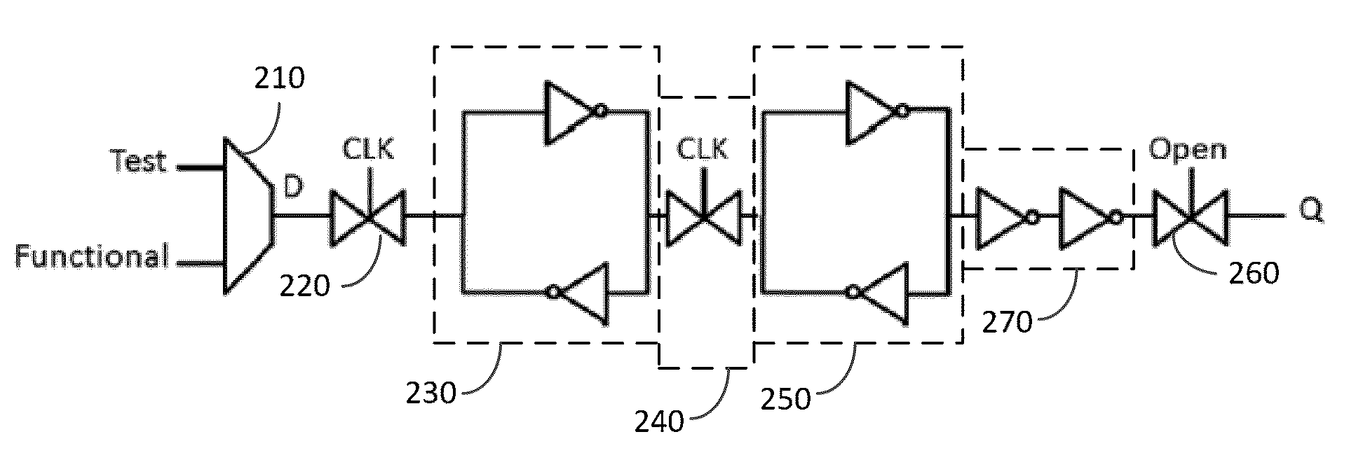
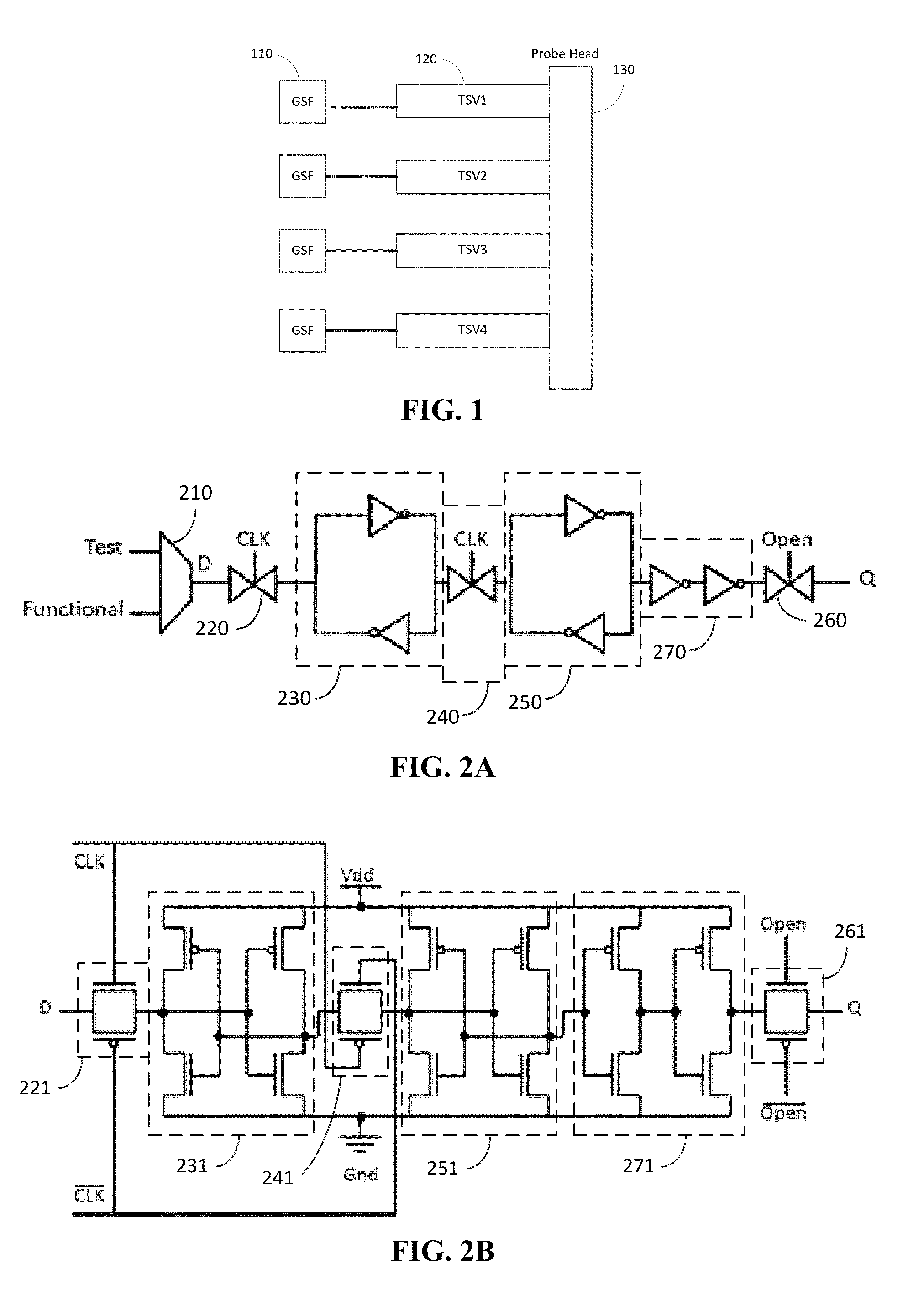
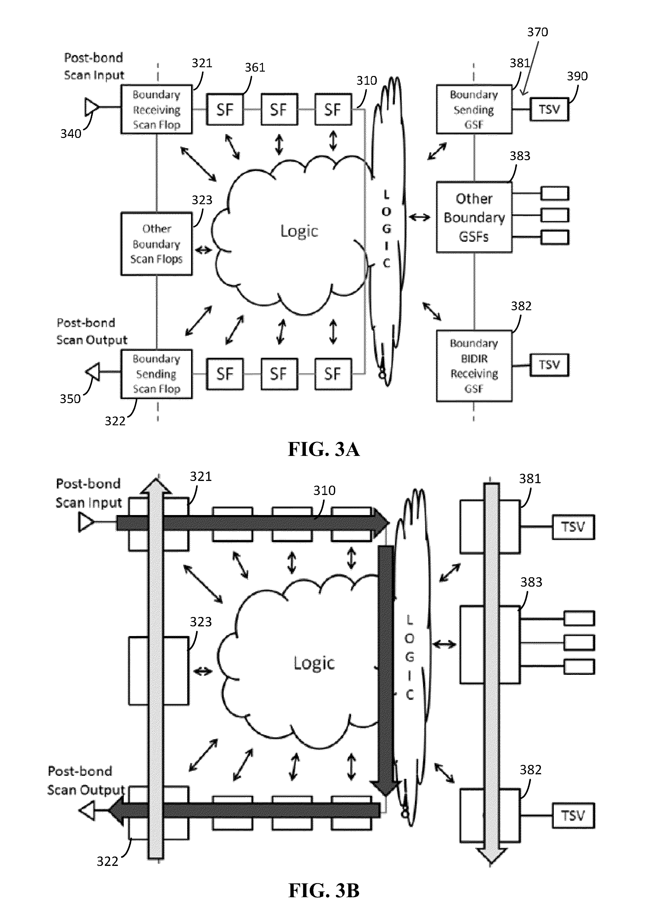
[0050]Simulations were conducted in HSPICE on a 3D logic-on-logic benchmark with 100 scan chains and using the configurations as illustrated in FIGS. 4A and 5.

[0051]For the examples, a 3D IC benchmark was created from a Fast Fourier Transform (FFT) circuit chosen from the OpenCores set of benchmarks. The FFT circuit is synthesized using the Nangate open cell library at the 45 nm technology node. The total gate count after synthesis is 299,273, with 19,962 flip-flops. The design was partitioned into 4 dies, with the gate counts in each die being 78,752; 71,250; 78,367; and 70,904, respectively. The logic gates in each die are placed using the CADENCE ENCOUNTER platform, a registered trademark of Cadence Design Systems, Inc., and TSVs are inserted in a regular fashion, using a minimum spanning tree approach. Back-to-face bonding is assumed, which means that TSVs are present only in the first three dies. The TSV counts are 936, 463, and 701, respectively. The TSV diameters in this chip...


PUM


Abstract

A test architecture for 3D ICs is provided in which Through-Silicon-Vias and die logic can be tested pre-bonding dies in the stack for the 3D ICs. Post-bond scan test architecture is reconfigured to be accessed during pre-bond testing through using stratigically placed MUXs and TSVs. By connecting post-bond architecture including scan flops and boundary registers to gated scan flops used in TSV testing, an internal chain of scan flops such as typically used in post-bond testing can be selectively connected to gated scan flops connected to one end of each TSV for pre-bond testing of the internal logic through the TSVs.

Description

[0001]This invention was made with government support under Federal Grant No. CCF-1017391 awarded by the National Science Foundation. The government has certain rights in the invention.BACKGROUND[0002]As semiconductor technology continues to scale, interconnect delay and power consumption threaten to limit the benefits of further scaling. To overcome these bottlenecks, the semiconductor industry is exploring 3D integration through die stacking and through-silicon-vias (TSVs).[0003]A TSV is a metal pillar that connects to a metal layer and is embedded in the device substrate. In a 3D stacked IC (SIC), two or more dies are produced with their own active device and metal layers and then bonded together with vertical TSVs connecting metal layers of adjacent dies. To expose the TSV pillar, much of the substrate is ground away in a process called “thinning” After thinning, metal balls called “microbumps” are added to the end of the TSV for use in bonding.[0004]Because of the move to verti...

Claims


Application Information

Patent Timeline
Patent Type & Authority Applications(United States)
IPC IPC(8): G01R31/3177
CPCG01R31/318558G01R31/318513G01R31/3177
Inventor CHAKRABARTY, KRISHNENDUNOIA, BRANDON
Owner DUKE UNIV
Why Eureka
Try Eureka