Probe card cooling assembly with direct cooling of active electronic components

a technology of active electronic components and cooling assembly, which is applied in the field of micro-onductors manufacturing and testing, can solve the problems of poor dies, difficult to provide uniform output signals, and poor dies, so as to reduce the conduction path of signals, increase performance, and facilitate disassembly for maintenance and repair.

Inactive Publication Date: 2005-05-10
FORMFACTOR INC
View PDF47 Cites 127 Cited by
  • Summary
  • Abstract
  • Description
  • Claims
  • Application Information

AI Technical Summary

Benefits of technology

[0021]An advantage of the present invention is that embodiments of the present invention can include a probe card cooling assembly for use in a test system which position a direct cooled package at or near probe elements. One or more dies can then carry out high-power applications such as testing operations at or near probe elements. Additional active electronic components can be included in one or more dies at or near probe elements without reaching an overheating condition that degrades testing signal quality to an unacceptable level. Placing the active electronic components at or near the probe elements rather than at a more remote tester also reduces the conduction path of signals and further increases performance. In one embodiment, a routine for positioning active electronic testing components near probe elements is provided. This routine includes sealing active components in a package, coupling the package to probe elements, and circulating coolant through the package during operation of the active components in testing.
[0022]One additional advantage of a probe card cooling assembly with direct cooling according to the present invention is it is easy to disassemble for maintenance and repair. Another advantage of the probe card cooling assembly with direct cooling according to the present invention is that it is inexpensive to assemble. Another advantage is that in certain embodiments electrical interconnects can be made to both the top and bottom of the package.
[0023]Further, in another embodiment of the present invention, a probe card cooling assembly according to the present invention includes a cooling member and a cooled package with one or more heat radiators such as cooling fins. The cooled package includes a housing that encloses a cavity. A coolant fills the cavity. One or more dies are mounted on a substrate within the cavity and are directly cooled by surrounding coolant. In this embodiment, however, heat is transferred away from the coolant by one or more heat radiators to the cooling member.
[0024]Further features and advantages of the present invention, as well as the structure and operation of various embodiments of the present invention, are described in detail below with reference to the accompanying drawings.
[0025]The accompanying drawings, which are incorporated herein and form part of the specification, illustrate the present invention and, together with the description, further serve to explain the principles of the invention and to enable a person skilled in the pertinent art to make and use the invention. In the accompanying drawings:
[0026]FIG. 1 is a side view of certain components in use in a conventional test system including a probe card and wafer.

Problems solved by technology

In practice, however, certain physical defects in the wafer itself and certain defects in the processing of the wafer inevitably lead to some of the dies being “good” (fully-functional) and some of the dies being “bad” (partially functional or non-functional).
These demands upon probe card assembly 140 make it more difficult to provide uniform output signals.
Problems such as pin-to-pin skew, differences in rise time, and other parasitics can occur as electrical signals travel through probe card assembly 140 during testing.
This solution can be of somewhat limited benefit, however, since the electrical path between probe elements 130 and PCB 230 may still be too great to sufficiently reduce parasitics.
Moving active electronic components close to probe elements 130, however, results in design problems heretofore not faced in probe card assemblies.
Among other things, this leads to a heating problem not encountered before in probe card assemblies.

Method used


Image

  • Probe card cooling assembly with direct cooling of active electronic components
  • Probe card cooling assembly with direct cooling of active electronic components
  • Probe card cooling assembly with direct cooling of active electronic components

Examples


Embodiment Construction

Table of Contents

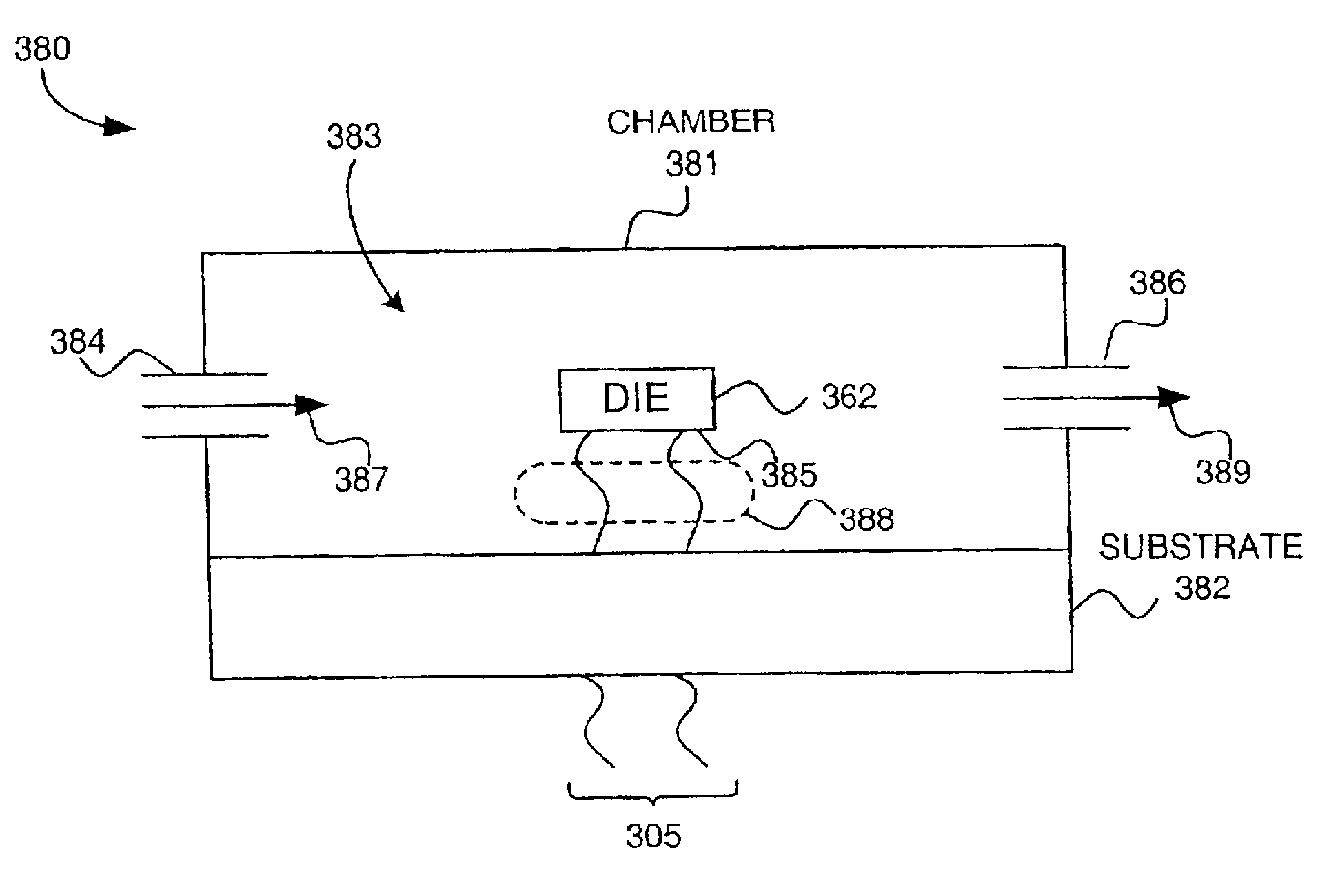
[0041]1. Overview and Discussion[0042]2. Terminology[0043]3. Probe Card Cooling Assembly[0044]4. Cooled Package with One or More Dies[0045]5. High-Density Cooled Packages[0046]6. Routine for Incorporating Active Electronic Components Near Probe Elements[0047]7. Types of Springs Contacts[0048]8. Additional Embodiments[0049]9. Conclusion

[0050]The following description is for the best modes presently contemplated for practicing the invention. This description is not to be taken in a limiting sense, but is made merely for the purpose of describing the general principles of the invention. The scope of the invention should be ascertained with reference to the claims. In the description of the invention that follows, like numerals or reference designators will be used to refer to like parts or elements throughout.

1. Overview and Discussion

[0051]The present invention provides a probe card cooling assembly. The probe card cooling assembly includes a cooled package with one o...


PUM


Abstract

A probe card cooling assembly for use in a test system includes a package with one or more dies cooled by direct cooling. The cooled package includes one or more dies with active electronic components and at least one coolant port that allows a coolant to enter the high-density package and directly cool the active electronic components of the dies during a testing operation.

Description

BACKGROUND OF THE INVENTION[0001]1. Field of the Invention[0002]The present invention relates to semiconductor manufacturing and testing. The present invention further relates to probe cards that are used to perform test and / or burn-in procedures on semiconductor devices.[0003]2. Related Art[0004]Individual semiconductor (integrated circuit) devices (dies) are typically produced by creating several identical dies on a semiconductor wafer, using known techniques of photolithography, deposition, and the like. Generally, these processes are intended to create a plurality of fully-functional integrated circuit devices, prior to singulating (severing) the individual dies from the semiconductor wafer. In practice, however, certain physical defects in the wafer itself and certain defects in the processing of the wafer inevitably lead to some of the dies being “good” (fully-functional) and some of the dies being “bad” (partially functional or non-functional). It is generally desirable to be...

Claims


Application Information

Patent Timeline
Patent Type & Authority Patents(United States)
IPC IPC(8): G01R31/28G01R1/067G01R1/073
CPCG01R31/2875G01R1/07385G01R1/06727G01R31/2891G01R31/2886
Inventor MILLER, CHARLES A.
Owner FORMFACTOR INC
Why Eureka
Try Eureka