Circuit board with optoelectronic component embedded therein

a technology of optoelectronic components and circuit boards, which is applied in the direction of optical elements, circuit optical details, instruments, etc., can solve the problems of increasing the conductivity, unable to achieve further increase of conductivity, and the difficulty of fabricating the higher-performance semiconductor, so as to reduce the difficulty of fabrication and increase the layout density of optical transmission elements. , the effect of improving the layout density of optical transmission elements

Active Publication Date: 2009-04-14
PHOENIX PRECISION TECH CORP
View PDF6 Cites 8 Cited by
  • Summary
  • Abstract
  • Description
  • Claims
  • Application Information

AI Technical Summary

Benefits of technology

[0016]Another objective of the present invention is to provide a circuit board with optoelectronic component embedded therein, to shorten the conduction path to lower the signal transmission loss, and to reduce the noise and increase the optoelectronic signal transmission quality.
[0025]Moreover, a heatsink board is further formed on a bottom surface of the carrier board or a heatsink block is formed on the non-active surface of the optoelectronic component, in order to diffuse the heat generated by the first and second optoelectronic components during operation to the outer environment efficiently, thereby strengthen the heat dissipation efficiency of the present invention of the circuit board with optoelectronic component embedded therein.

Problems solved by technology

The straightest way to increase the processing rate of processor is to increase the operating frequency, but facing bottlenecks such as heat dissipation for high power, delay of signal time and electric magnetic interruption (EMI) when the data transmission is above Gb / s, which makes the fabrication of the higher performance semiconductor more difficult.
Especially when the copper circuit is conventionally used as a carrier for data transmission, with the natural conductivity limitation of this material, the achieved conductivity cannot be further increased, therefore the signal transmission rate cannot be increased by increasing the conductivity.
In addition, the metallic circuit structure for signal transmission is easy to have interruption form the outside noise or interference form the inner circuit, results in signal transmission error due to the interruption and interference during the signal transmission process; therefore, some protection methods are required for the signal transmission structure to prevent the interruption and interference occur to affect the signal, especially obvious in the high frequency transmission.
The protection methods have increased some difficulties and extra structure design for the circuit design, results in increasing in the design cost and the fabrication cost, and therefore, the present condition is hard to make a breakthrough.
Moreover, the conventional signal transmission method is an analogue signal transmission method using electricity flowing through the conductor, but the signal processing methods inside the circuits nowadays mostly are digital processing; therefore a distortion may occur after conversion during the transmission process.
An automatic placing movement, like the conventional insertion movement when inserting electronic components into circuit board, completes the fabrication process of placing the optical fiber 13 into the groove 12a; therefore the speed of the fabrication is slow, and cannot achieve the rapid production purpose.
Moreover, the optical fiber 13 needs to be cut first according to the corresponding groove 12a length, and then places the optical fiber 13 into the groove 12a, which adds another process in the fabrication, therefore increases the fabrication difficulty; and the optical fiber 13 has different lengths, thereof increases the fabrication assorting difficulties, leads to the addition of complexity of the whole fabrication process, and consequently increases the fabrication cost.
The optical fiber 13 and the circuit board have different fabrication structure, thus needs to be fabricated by another independent fabrication process and increases difficulty of the whole fabrication process; and to integrate the two different fabrication products increase difficulty as well, thus cannot achieve the mass production purpose to lower the fabrication cost.
Thus, the increasing fabrication difficulty and cost due to optical fiber 13 has to be embedded in the saturated layer 12, and further, failing to meet the high density optical transmission element layout requirements, has become problems for industries desired to be resolved.

Method used


Image

  • Circuit board with optoelectronic component embedded therein
  • Circuit board with optoelectronic component embedded therein
  • Circuit board with optoelectronic component embedded therein

Examples


first embodiment

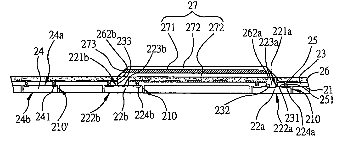
[0040]Referring to FIG. 2A, which is a cross-sectional diagram, illustrating the first embodiment of the present invention of the circuit board with optoelectronic component embedded therein, comprises: a carrier board 21 with at least two through openings 210, and the first and second optoelectronic components 22a, 22b are disposed in the openings 210 respectively; an dielectric layer 23 formed on the surface of the carrier board 21, the first and second optoelectronic components 22a, 22b; and a circuit layer 25 formed on the surface of the dielectric layer 23.

[0041]The carrier board 21 could be metal board, ceramic board, insulating board and organic circuit board, or any board mentioned here forming a stack structure freely; therein the organic circuit board is printed circuit board or IC packaging substrate. The use of metal board or ceramic board can be used as a heatsink for the first and second optoelectronic components 22a, 22b, or using the organic circuit board as the carr...

second embodiment

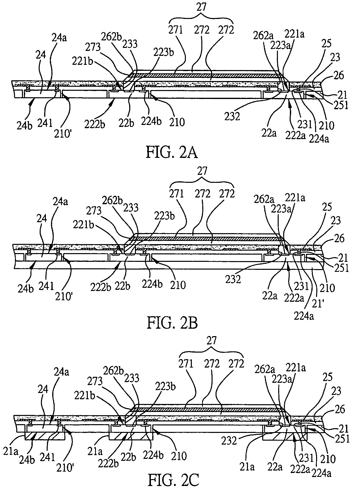
[0049]Referring to FIG. 2B, which is a cross-sectional diagram, illustrating the second embodiment of the present invention of the circuit board with optoelectronic component embedded therein, has a difference comparing to the previous embodiment. Another carrier board 21′ is attached to the bottom surface of the carrier board 21, and the carrier board 21′ could be metal board, ceramic board, insulating board and organic circuit board, or any board mentioned here forming a stack structure freely; therein the organic circuit board is printed circuit board or IC packaging substrate; and if the carrier board 21′ is made form metal board or ceramic board, the heat generated by the first and second optoelectronic components 22a, 22b and the semiconductor component 24 during operation can be diffused effectively, which strengthen the heat dissipation efficiency of the circuit board with optoelectronic component embedded therein.

[0050]Referring to FIG. 2C, a heatsink block 21a is disposed ...

third embodiment

[0051]Referring to FIG. 2D, a cross-sectional diagram illustrating the third embodiment of the present invention of the circuit board with optoelectronic component embedded therein, has a difference comparing to the previous embodiment, where a protecting shield such as an encapsulant 28 is formed on the optical transmission element 27 and the insulating protecting layer 26, to protect the optical transmission element 27 from damage by the outside influence, thereby increases the lifetime of the product.

[0052]Referring to FIG. 2E illustrating another embodiment of the optical transmission element protection of the present invention, where a protecting shield such as metallic case 28′ is formed on the optical transmission element 27 and the insulating protecting layer 26, to protect the optical transmission element 27.


PUM


Abstract

A circuit board structure with optoelectronic component embedded therein comprises a carrier board with at least two through openings; a first optoelectronic component and a second optoelectronic component disposed in the openings respectively, wherein a plurality of electrode pads and optical active areas are formed on the active surfaces of the optoelectronic components; a dielectric layer formed on a surface of the carrier board and the active surface of the optoelectronic components, wherein a plurality of vias for exposing the electrode pads and two holes for exposing the optical active areas are formed in the dielectric layer; a circuit layer formed on a surface of the dielectric layer and electrically connected to the electrode pads of the optoelectronic components; an insulating protecting layer formed on the dielectric layer and the circuit layer; and at least one optical transmission element formed on a surface of the insulating protecting layer.

Description

CROSS-REFERENCE TO RELATED APPLICATION[0001]This application claims benefit under 35 USC 119 to Taiwan Application No. 094139383, filed Nov. 10, 2005.FIELD OF THE INVENTION[0002]The present invention relates to an integration of circuit and optoelectronic component structure, and, more particularly, to a circuit with optoelectronic component embedded therein.BACKGROUND OF THE INVENTION[0003]With the highly increasing development in the electrical industries, the direction of the research and design for the electronic products has gradually shifted to multi-function and high performance. In order to satisfy the packaging requests of integration and miniaturization for the semiconductor packaging, the circuit board that carrying a plurality of the active, non-active components and the circuits has evolved to multi-layer board gradually.[0004]The development of semiconductor technology improves day by day rapidly, besides mainly focusing on the tiny packaging of the model, nowadays the...

Claims


Application Information

Patent Timeline
Patent Type & Authority Patents(United States)
IPC IPC(8): G02B6/12G02B6/26H01S3/04
CPCG02B6/43H05K1/0274H05K1/185H01L2224/04105H01L2224/73267H01L2924/18162
Inventor HSU, SHIH-PING
Owner PHOENIX PRECISION TECH CORP
Why Eureka
Try Eureka