Back passivation matrix dot type laser grooving conductive structure

A rear passivation and laser slotting technology, which is applied in photovoltaic power generation, circuits, electrical components, etc., can solve the problem of laser slotting areas that cannot completely fill a single circular hole-shaped spot, and the large volume of inorganic adhesives and additives mixed , It is not conducive to the collection of photogenerated carriers, etc., to achieve the effect of improving photoelectric conversion efficiency and component reliability, facilitating collection, and improving transmission and collection capabilities

Active Publication Date: 2018-10-16
TONGWEI SOLAR (ANHUI) CO LTD
View PDF8 Cites 7 Cited by
  • Summary
  • Abstract
  • Description
  • Claims
  • Application Information

AI Technical Summary

Problems solved by technology

[0008] The diameter of the round hole-shaped spot of the laser groove is too small, and the particle size of the Al powder that burns through the aluminum paste on the back passivation layer is generally 4-12um, and the mixing volume of the organic carrier, inorganic adhesive and additive is too large , the laser grooved area that cannot completely fill a single circular hole-like spot is easily formed after the slurry is dried and sintered in the later stage. The contact cavity 7 between the conductive aluminum paste 6 and the silicon wafer substrate 1 on the back, as shown in the attached manual Figure 5 As shown, the export of photo-generated carriers generated in the PN junction region is limited, and the conduction resistance increases, which is not conducive to the collection of photo-generated carriers in the direction of the back plane, and will not form a complete local aluminum back field structure.

Method used


Image

  • Back passivation matrix dot type laser grooving conductive structure
  • Back passivation matrix dot type laser grooving conductive structure
  • Back passivation matrix dot type laser grooving conductive structure

Examples


Embodiment

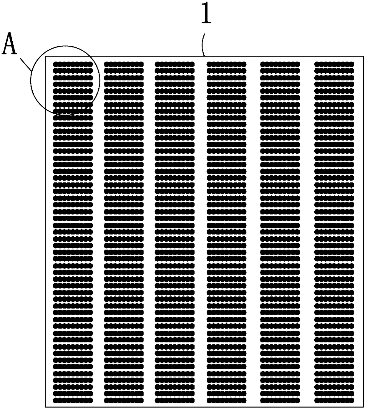
[0040] After front-side texturing, diffusion, cleaning to remove PSG, and backside polishing, removing the back surface of the PN junction polysilicon wafer substrate 1 at the boundary, annealing to form a 2nm SiO2 film, ALD deposition of A2O3 3nm, PECVD deposition of Si3N4 130nm, forming a total thickness of 135nm After stacking the passivation film 2 on the backside, it is turned over, and a silicon nitride anti-reflection passivation protective film layer is deposited on the front surface PN junction region of the silicon wafer substrate 1 by PECVD.

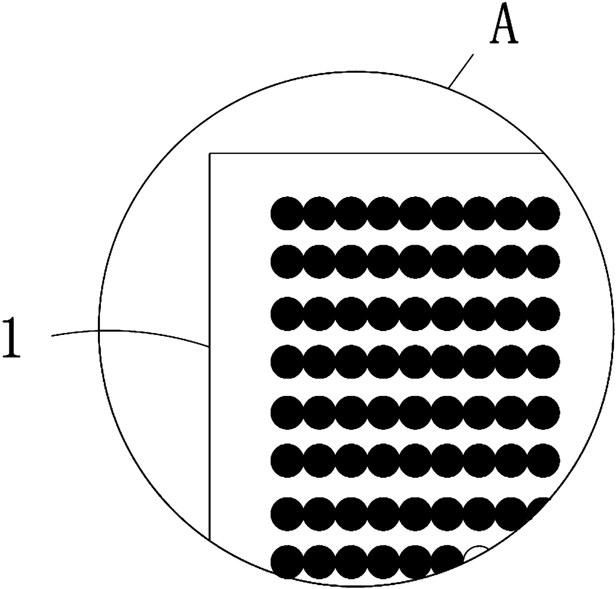
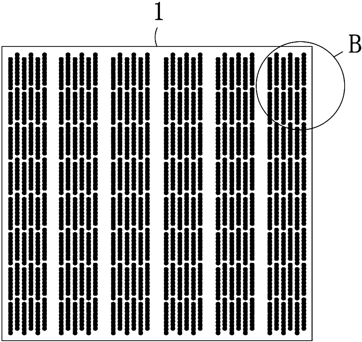
[0041] Five four-segment back electrode busbar regions 3 are arranged on the backside passivation film 2 of the stack, with a length of 18mm and a width of 2.2mm. The backside electrode is to be screen-printed and is 1.5mm away from the edge of the silicon wafer substrate 1. Laser drilling and grooving are not carried out in the inner area, and laser drilling and grooving are used in other areas.

[0042] On the back surface o...


PUM


Abstract

The invention discloses a back passivation matrix dot type laser grooving conductive structure. The structure comprises a silicon wafer substrate, wherein the back face of the silicon wafer substrateis provided with lamination back passivation film, and back electrode main gate regions are arranged at intervals on the lamination back passivation film; laser grooving is carried out on non-back electrode main gate regions on the lamination back passivation film through a lamination back passivation film in a wave band of 500-1200 nanometers to from a repeating dot group structure unit, whereinthe repeating point group structure unit is composed of 2-18 circular-aperture-shaped laser spots overlapping 3%-17% of a circular area region, and the intervals of center points of the repeating point group structure unit are 0.2-1.0 millimeters. The laser grooving conductive structure has the advantage that a back conduction plane can be divided into smaller conductive structure units, so that the photo-generated current conduction path is shortened, the transmission collecting capacity of current carriers is improved, lattice damage and composite damage of the battery silicon wafer substrate caused by the laser grooving can be reduced, and the photovoltaic conversion efficiency and assembly reliability of single polycrystalline silicon back passivation local back contact solar cell areimproved.

Description

technical field [0001] The invention relates to the technical field of backside passivation of silicon wafers, in particular to a backside passivation matrix dot-type laser slotted conductive structure. Background technique [0002] The main efficiency range of conventional single polycrystalline silicon solar cells is 18.6-20.3%. In order to further improve the photoelectric conversion efficiency of crystalline silicon cells, a passivation layer is added on the back of the cell. The efficiency of the battery is increased to 19.3-21.7%, and the corresponding component power generation output power is also greatly improved. [0003] Compared with the conventional single polycrystalline cell process, the backside passivation localized back contact single polycrystalline cell mainly adds three processes: backside passivation, backside SiNx film deposition and laser drilling and slotting. Among them, the laser drilling and grooving process uses a laser with a certain pulse widt...

Claims


Application Information

Patent Timeline
Patent Type & Authority Applications(China)
IPC IPC(8): H01L31/0216H01L31/0224
CPCH01L31/02167H01L31/022441Y02E10/50
Inventor 王岚杨蕾张元秋常青吴俊旻张冠伦
Owner TONGWEI SOLAR (ANHUI) CO LTD
Why Eureka
Try Eureka