Package structure in which coreless substrate has direct electrical connections to semiconductor chip and manufacturing method thereof

a coreless substrate and semiconductor chip technology, applied in the direction of semiconductor devices, semiconductor/solid-state device details, electrical apparatus, etc., can solve the problems of many limitations in this technique, inability to achieve electrical connections, etc., to achieve the effect of simplifying manufacturing

Active Publication Date: 2011-11-15
UNIMICRON TECH CORP
View PDF15 Cites 8 Cited by
  • Summary
  • Abstract
  • Description
  • Claims
  • Application Information

AI Technical Summary

Benefits of technology

[0011]The object of the present invention is to provide a package structure in which a coreless substrate has direct electrical connections to a semiconductor chip and a method for manufacturing the same, so that connection between the semiconductor chip and the coreless substrate, and formation of the conductive structures thereof can be integrated together. Hence, simplification of the manufacturing can be achieved.
[0012]Another object of the present invention is to provide a package structure in which a coreless substrate has direct electrical connections to a semiconductor chip and a method for manufacturing the same so that the flexibility of fine circuit layouts can be promoted, and the reduction of conductive paths can be achieved. Consequently, the electrical properties of semiconductor devices can be promoted.
[0013]Furthermore, another object of the present invention is to provide a package structure in which a coreless substrate has direct electrical connections to a semiconductor chip and a method for manufacturing the same so that the thinned packaging substrate can be effective in decreasing the whole thickness of the semiconductor package structure. Therefore, the desired compact and lightweight electronic products can be made.

Problems solved by technology

However, even though the purpose of high quantity pin counts can be achieved through the method illustrated above, the electrical performance of a device operated in higher frequency or at higher speed can be unavailable or limited due to the long paths of conductive circuits.
Even though a flip chip ball grid array packaging substrate could meet the requirement of high quantity pin counts and be used in a device operated in high frequency, there are many limitations in this technique, especially regarding electrical connections.
Furthermore, other alternative materials still have electrical and mechanical problems, such as unstable quality of connections, and those problems are still awaiting solutions.
However, resin is viscous and does not easily flow into the gap, thus the finer the circuits of a packaging substrate, the longer the time needed for filling with the resin.
Additionally, there are many unfilled voids in the resin filled region, resulting in increased risk of bust-up of the package structure.
However, the formed plated through holes 124 compromise the flexibility of the fine circuit layout.
Hence, reduction of conductive paths in the substrate 12 is limited, and the electrical characteristics could not be well improved.
Furthermore, the thickness of the substrate 12 could not be decreased efficiently because of the existence of the core layer 120.
On the other hand, if the core layer 120 is thinned to 60 μm or less, it is difficult to produce the substrate 12, and further results in great reduction in the yield of the substrate 12.
Therefore, the core layer 120 does not favor reduction of the whole thickness of the package structure, thus the demands of compact and lightweight electronic devices have not been met.
These steps of the manufacturing are complex and not easily simplified.

Method used


Image

  • Package structure in which coreless substrate has direct electrical connections to semiconductor chip and manufacturing method thereof
  • Package structure in which coreless substrate has direct electrical connections to semiconductor chip and manufacturing method thereof
  • Package structure in which coreless substrate has direct electrical connections to semiconductor chip and manufacturing method thereof

Examples


embodiment 1

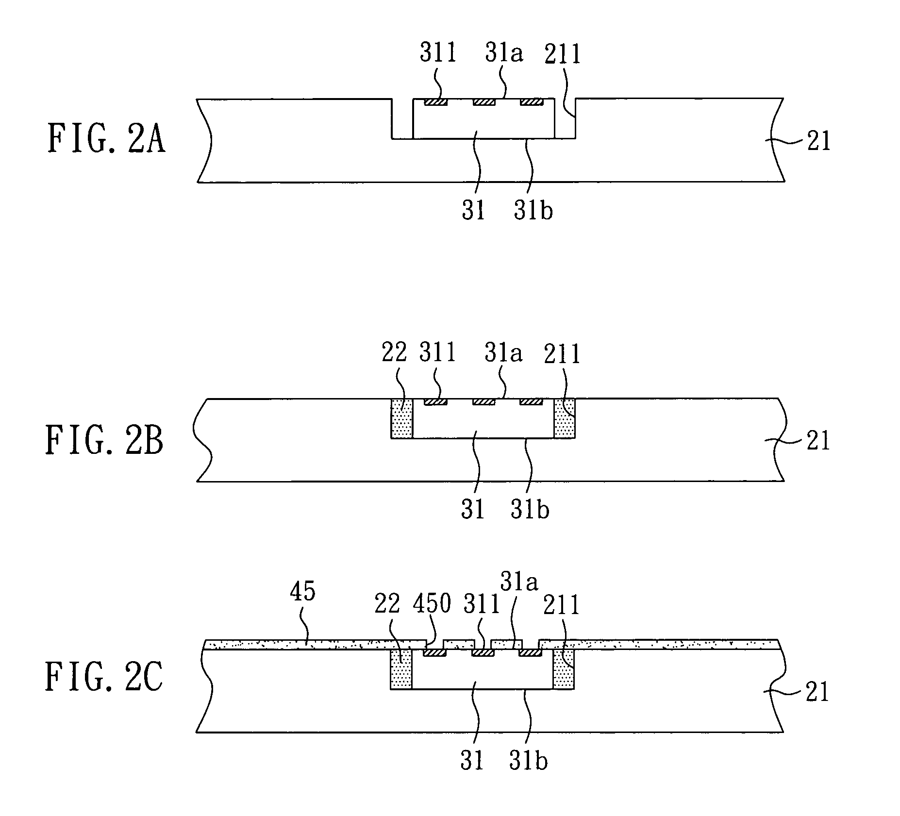
[0034]First, as shown in FIG. 2A, a metal carrier board 21 having at least one cavity 211 is provided. The metal carrier board 21 can be made of Al, Cu, Fe, or an alloy thereof. In detail, the cavity 211 is formed through etching. Then, a semiconductor chip 31 is disposed in the cavity 211 of the metal carrier board 21. The semiconductor chip 31 has an active surface 31a and an opposite inactive surface 31b. The active surface 31a of the semiconductor chip 31 has a plurality of electrode pads 311 thereon. In addition, the inactive surface 31b of the semiconductor chip 31 faces the cavity 211 of the metal carrier board 21 so that the semiconductor chip 31 is placed therein. In particular, the inactive surface 31b of the semiconductor chip 31 is temporarily fixed on the bottom of the cavity 211 by an adhesive material (not shown). The semiconductor chip 31 can be an active component or a passive component. The passive component can be a resistor, a capacitor, or an inductance.

[0035]Su...

embodiment 2

[0040]With reference to FIGS. 3 and 3-1, the present Embodiment has some differences as compared to Embodiment 1, listed as follows. While removing the metal carrier board 21, a part of the metal carrier board 21 is not removed so that a part of the first solder mask 45 is exposed. The remaining part of the metal carrier board 21 serves as a metal supporting frame 21′. Hence, the rigidity of the built-up structure 5 can be enhanced. Other steps are the same as those of Embodiment 1, and are not illustrated again. The differences between FIGS. 3 and 3-1 can be known with reference to the illustrations of FIGS. 2D and 2D-1.

embodiment 3

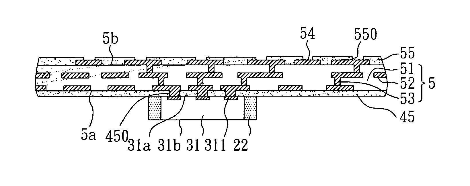
[0041]The present Embodiment has some differences as compared to Embodiment 1, explained by the following. With reference to FIG. 4A, the built-up structure 5 is first formed on the surface of the metal carrier board 21 and on the active surface 31a of the semiconductor chip 31. Then, the metal carrier board 21 is totally removed. As shown in FIG. 4B, the first solder mask 45 can be formed by stencil printing etc. on the uncovered region of the surface with the semiconductor chip31 disposed thereon of the built-up structure 5 because the properties (like the relatively high hygroscopicity) of the dielectric material used as the dielectric layer 51 of the built-up structure 5 may be sensitive to the environment. As a result, the manufacturing of the present invention is accomplished.

[0042]The present invention further provides a package structure of a coreless substrate with direct electrical connections to a semiconductor chip, which comprises a semiconductor chip 31, a built-up str...


PUM


Abstract

A package structure in which a coreless substrate has direct electrical connections to a semiconductor chip and a manufacturing method thereof are disclosed. The method includes the following steps: providing a metal carrier board having a cavity; placing a chip having a plurality of electrode pads on an active surface in the cavity of a board; filling the cavity with an adhesive for fixing the chip; forming a solder mask on the active surface of the chip and the surface of the metal carrier board at the same side, wherein the solder mask has a plurality of openings to expose the electrode pads of the chip; forming a built-up structure on the solder mask and the exposed active surface of the chip in the openings; and removing the metal carrier board. In this method the metal carrier board can support the built-up structure to thereby avoid warpage.

Description

BACKGROUND OF THE INVENTION[0001]1. Field of the Invention[0002]The present invention relates to a package structure and a manufacturing method thereof. In more detail, the present invention relates to a package structure and a manufacturing method thereof in which a coreless substrate with circuits has direct electrical connections to a semiconductor chip.[0003]2. Description of Related Art[0004]As the electronics industry develops rapidly, research moves towards electronic devices with multiple functions and high performance. Hence, circuit boards with many active and passive components and circuit connections integrated therein have advanced from being single-layered boards to multi-layered boards by an interlayer connection technique, so as to expand circuit layout space in a limited circuit board to thereby meet the demand of the application of high-density integrated circuits.[0005]With regard to conventional semiconductor package structures, a chip is mounted on the top surfa...

Claims


Application Information

Patent Timeline
Patent Type & Authority Patents(United States)
IPC IPC(8): H01L23/52
CPCH01L21/6835H01L24/19H01L24/24H01L23/5389H01L2224/0401H01L2221/68345H01L2221/68359H01L2224/04105H01L2224/16227H01L2224/20H01L2224/24227H01L2924/01013H01L2924/01029H01L2924/01082H01L2924/14H01L2924/15153H01L2924/15165H01L2924/15311H01L2924/19041H01L2924/19043H01L2924/30107H01L2924/1815H01L2224/16225H01L2924/01033H01L2224/32245H01L2224/73267H01L2924/18162
Inventor CHIA, KAN-JUNG
Owner UNIMICRON TECH CORP
Why Eureka
Try Eureka