Semiconductor device integrated with optoelectronic components

Active Publication Date: 2007-05-10
PHOENIX PRECISION TECH CORP
View PDF7 Cites 8 Cited by
  • Summary
  • Abstract
  • Description
  • Claims
  • Application Information

AI Technical Summary

Benefits of technology

[0023] Therefore, the present invention of the semiconductor device integrated with optoelectronic components mainly comprises a carrier board with at least two openings; a first optoelectronic component and a second optoelectronic component disposed in the openings respectively, each of the first and second optoelectronic components having an active surface and an opposite non-active surface, wherein the active surface has a plurality of electrode pads and an optical active area; a dielectric layer formed on a surface of the carrier board and the active surfaces of the first and second optoelectronic components, the dielectric layer having a plurality of vias to expose the electrode pads of the first and second optoelectronic components and a plurality of openings to expose the optical active areas of the first and second optoelectronic components; and a circuit layer formed on a surface of the dielectric layer, and electrically connected to the electrode pads of the first and second optoelectronic components by electrical conductive structures formed in the vias of the dielectric layer. In addition, let the optical active areas of the first and second optoelectronic components correspond to the openings of the

Problems solved by technology

The straightest way to increase the semiconductor's processing rate is to increase the utilization ratio, but facing bottlenecks such as heatsink for high power, delay of signal time and electric magnetic interruption (EMI) when the data transmission is above Gb/s, which makes the fabrication of the higher performance semiconductor more difficult.
Especially when the copper circuit is conventionally used as a carrier for data transmission, with the limitation of this material's natural conductivity, the achieved conductivity cannot be increased further, therefore the signal transmission rate cannot be increased by increasing the conductivity.
In addition, the metallic circuit structure for signal transmission is easy to have interruption from the outside noise or interference from the inner circuit, results in signal transmission error due to the interruption and interference during the signal transmitting process; therefore, some protection methods are required for the signal transmission structure to prevent the interruption and interference occur to affect the signal, especially obvious in the high frequency transmission.
The protection methods have increased some difficulties and extra structure design for the circuit design, results in increasing in the design cost and the fabrication cost, and therefore, the present condition is hard to make a breakthrough.
Moreover, the conventional signal transmission method is an analogue signal transmission method using electric current through the conductor, but the signal processing metho

Method used


Image

  • Semiconductor device integrated with optoelectronic components
  • Semiconductor device integrated with optoelectronic components
  • Semiconductor device integrated with optoelectronic components

Examples


first embodiment

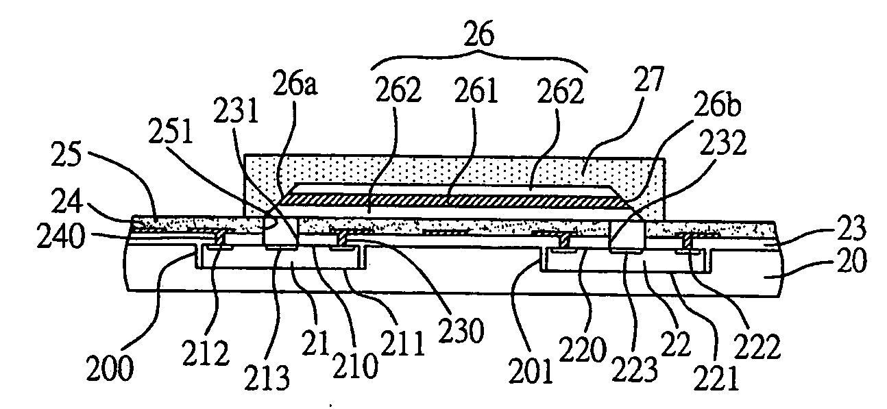
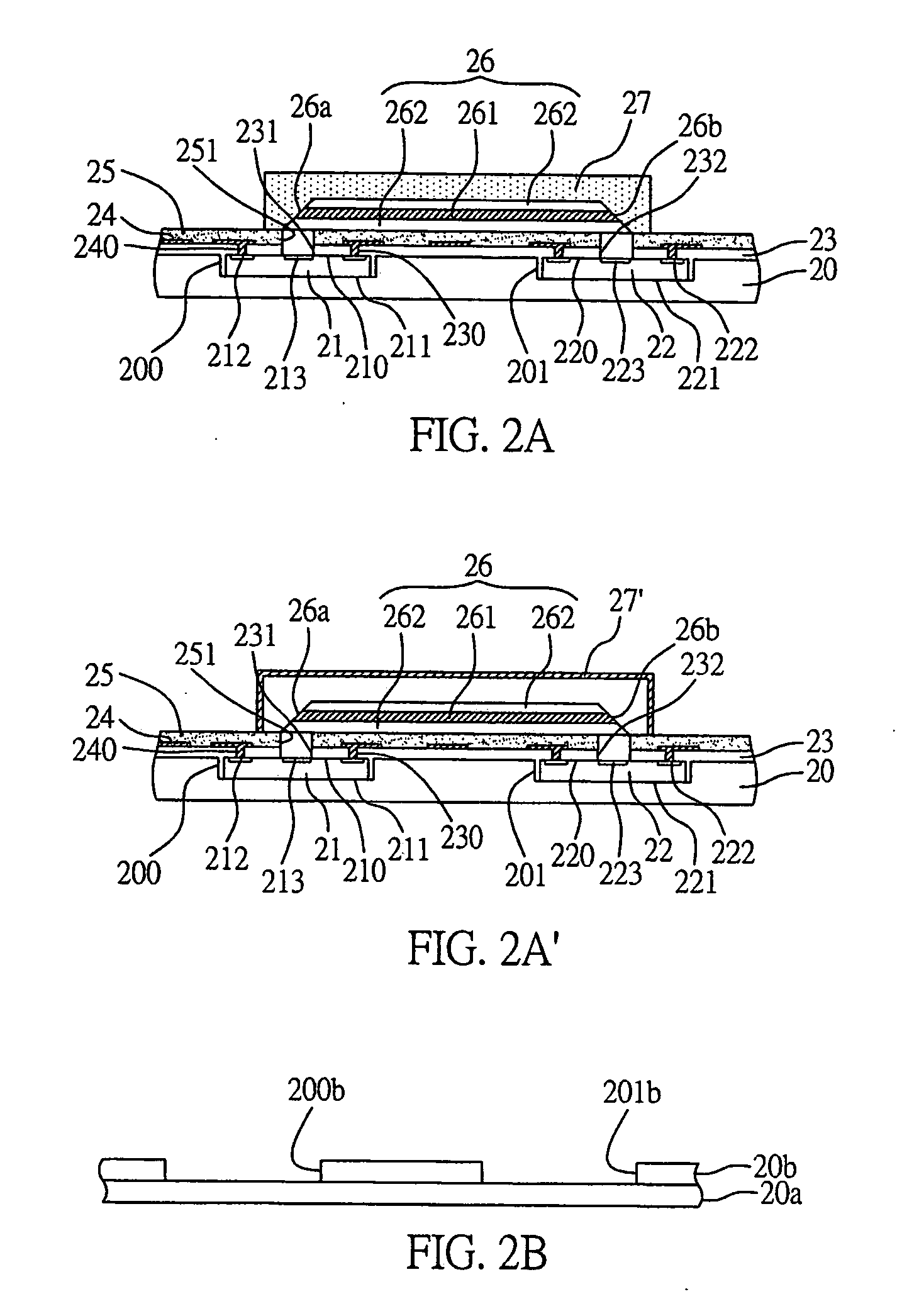
[0036] Referring to FIG. 2A, it is a cross-sectional diagram, illustrating the first embodiment of the present invention of a semiconductor device integrated with optoelectronic components.

[0037] As shown in the diagram, the optoelectronic component integrated in semiconductor device, comprises: a carrier board 20 with at least two openings 200, 201 that are not penetrating the carrier board; a first and a second optoelectronic components 21, 22 disposed in the openings respectively; a dielectric layer 23 formed on a surface of the carrier board 20 and active surface of the first and second optoelectronic components 21, 22; and a circuit layer 24 formed on the dielectric layer 23 and electrically connected to the first and second optoelectronic components 21, 22.

[0038] The carrier board 20 is an integrally formed heat sink and is made of one of metal and a ceramic material.

[0039] Beside, the carrier board 20 can be composed by stacking a plurality of carrying layers. Below is the...

second embodiment

[0050] As shown in FIG. 3A, it is a cross-sectional diagram, illustrating the second embodiment of the present invention of a semiconductor device integrated with optoelectronic components.

[0051] The semiconductor device integrated with optoelectronic components of the present embodiment is roughly the same with previous described first embodiment, the main differences of the semiconductor device integrated with optoelectronic components of the present embodiment is, further includes at least one waveguide 26′ formed on the surface of the insulating layer 25, and the waveguide 26′ has a transmission terminal 26a′ with a reflection surface; the transmission terminal 26a is facing to the optical active area 223 of the second optoelectronic component 22 to let the second optoelectronic component 22 transmit the signal to other optoelectronic components via the waveguide 26′, thereof expands the product's capacity.

[0052] Referring to FIGS. 3B and 3B′, the insulating layer 25 and the w...

third embodiment

[0053] As shown in FIG. 3B, it is a cross-sectional diagram, illustrating the third embodiment of the present invention of a semiconductor device integrated with optoelectronic components.

[0054] The semiconductor device integrated with optoelectronic components of the present embodiment is roughly the same with previous described second embodiment, the main differences of the semiconductor device integrated with optoelectronic components of the present embodiment is, further includes a circuit build-up fabrication to form a circuit build-up structure 31 on the dielectric layer 23 and the circuit layer 24, and forms openings 31a, 31b in the circuit build-up structure 31 at locations corresponding to the optical active areas 213, 223 of the first and second optoelectronic components 21, 22 to expose the optical active areas 213, 223 of the first and second optoelectronic components 21, 22, and then the circuit build-up structure 31 is further formed with an insulating layer 25 on the...


PUM


Abstract

A semiconductor device integrated with optoelectronic components includes a carrier board with at least two openings; a first and a second optoelectronic component disposed in the openings respectively, each of them having an active surface and an opposite non-active surface, wherein the active surface has a plurality of electrode pads and an optical active area; a dielectric layer formed on a surface of the carrier board and the active surfaces, and having a plurality of vias and openings to expose the electrode pads and the optical active areas respectively; and a circuit layer formed on a surface of the dielectric layer and electrically connected to the electrode pads directly. Then, at least one waveguide is formed on the surface of the semiconductor device integrated with the optoelectronic component to provide signal transmitting between the first and second optoelectronic components, therefore, shortens the signal transmission path, reduces the transmission loss and noise, and hence improves the signal transmission quality.

Description

CROSS-REFERENCE TO RELATED APPLICATION [0001] This application claims benefit under 35 USC 119 to Taiwan Application No. 094139069, filed Nov. 8, 2005. FIELD OF THE INVENTION [0002] The present invention relates to semiconductor devices integrated with optoelectronic components, and, more particularly, to a semiconductor device having optoelectronic components, a waveguide and a circuit structure. BACKGROUND OF THE INVENTION [0003] The development of semiconductor technology improves day by day rapidly, besides mainly focusing on the tiny packaging of the model, nowadays the data storage capacity is increasing gradually also. Therefore, with the increasing data quantity, the least time taken to process the same quantity data shows a higher efficiency in data processing. The straightest way to increase the semiconductor's processing rate is to increase the utilization ratio, but facing bottlenecks such as heatsink for high power, delay of signal time and electric magnetic interruptio...

Claims


Application Information

Patent Timeline
IPC IPC(8): G02B6/12G02B6/26
CPCG02B6/42G02B6/4214H01L23/48H01L24/18H01L24/82H01L2224/18H01L2924/01029H01L2924/15153H01L2924/15165H01L2924/3025H05K1/0274H05K1/185H01L2924/01033H01L2924/014H01L24/19H01L2224/04105H01L2224/32225H01L2224/32245H01L2224/73267H01L2224/92244H01L2924/12041H01L2924/00
Inventor HSU, SHIH-PING
Owner PHOENIX PRECISION TECH CORP
Why Eureka
Try Eureka