Wiring board for having light emitting element mounted thereon

A technology for light-emitting elements and wiring substrates, which can be applied to electrical components, circuit devices, and electrical solid-state devices, etc., and can solve the problems of obstructing the optical path, low luminous efficiency, and obstructing the optical path of the light-emitting element.

Inactive Publication Date: 2014-07-30
NGK SPARK PLUG CO LTD
View PDF6 Cites 8 Cited by
  • Summary
  • Abstract
  • Description
  • Claims
  • Application Information

AI Technical Summary

Problems solved by technology

However, as in the above-mentioned insulating substrate of Patent Document 1, when the mounting portion of the light-emitting element and the mounting portion of the protection element are provided on the same surface of the plate-shaped wiring board, the mounted protection element hinders the emission of the light-emitting element. The optical path of the light, or the light radiated in the hemispherical direction is polarized, so the luminous efficiency may be reduced
And, as in the above-mentioned Patent Document 1 Figure 4 As shown in the form shown, the mounting portion of the protective element is provided on the bottom surface of the concave portion that is opened in the peripheral portion of the surface of the insulating base. The optical path is obstructed in the vicinity of the above-mentioned concave portion, and the polarization of light occurs between the vicinity of the concave portion and other parts.

Method used


Image

  • Wiring board for having light emitting element mounted thereon
  • Wiring board for having light emitting element mounted thereon
  • Wiring board for having light emitting element mounted thereon

Examples


Embodiment Construction

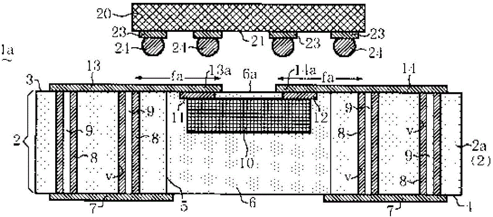
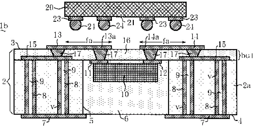
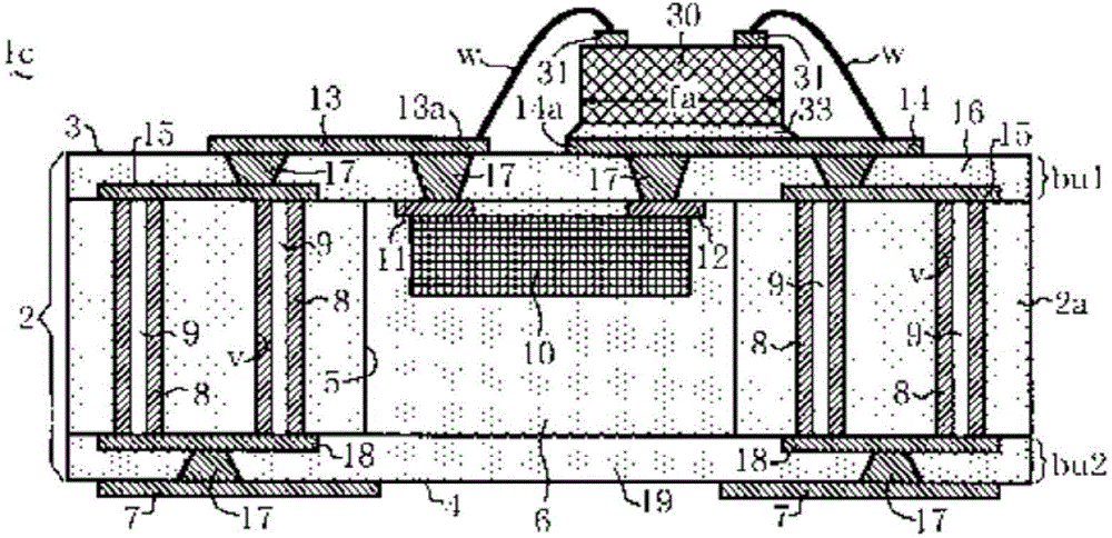
[0026] Embodiments for carrying out the present invention will be described below. figure 1 It is a vertical cross-sectional view showing a wiring board 1 a for mounting a light emitting element and a light emitting diode (light emitting element) 20 mounted on the wiring board 1 a for mounting a light emitting element according to an embodiment of the present invention. like figure 1 As shown, the wiring substrate 1a for mounting light-emitting elements includes: a substrate body 2 having a surface 3 and a back surface 4 and having a plate shape as a whole; a pair (multiple) of element terminals 13, 14 formed on the substrate body 2 A pair of external connection terminals 7, 7 formed on the back surface 4 of the substrate body 2; and a Zener diode (built-in component) 10 built in the substrate body 2. The substrate main body 2 is composed of a core substrate (insulating substrate) 2 a made of hard resin or ceramics and having a thickness of about 30 μm to 1000 μm. Hard resin...


PUM


Abstract

Provided is a wiring board for having a light emitting element mounted thereon, which has, on a front surface of a substrate main body having the front surface and a rear surface, a light emitting element mounting section, and an integrated component to be electrically connected to the light emitting element, and which does not generate, due to the integrated component, disturbance to optical path and polarization of light emitted from the light emitting element. A wiring board (1a) for having a light emitting element mounted thereon includes: a substrate main body (2), which has a front surface (3) and a rear surface (4), and which includes at least an insulating substrate (2a); and a plurality of element terminals (13, 14), which are formed on the front surface (3) of the substrate main body (2), and at least one of which has a light emitting element mounting section (fa) on an upper surface. The wiring board (1a) has a zener diode (integrated component) (10) integrated in the substrate main body (2) by having the zener diode embedded therein, said zener diode to be electrically connected to a light emitting element (20) to be mounted on the mounting section (fa), and preventing overvoltage from being applied to the light emitting element (20).

Description

technical field [0001] The present invention relates to a wiring board for mounting a light-emitting element on a surface of a board main body. Background technique [0002] For example, a light-emitting element housing package is proposed, which includes: a mounting portion of a light-emitting element such as a light-emitting diode, and a mounting portion of a protection element for preventing the light-emitting element from being applied with an overvoltage; A wiring conductor between the two elements; and a reflective member mounted on the surface (one main surface) of the insulating base, the inner peripheral surface of the reflective member is a light reflective surface, and the reflective member surrounds the mounting portion of the above-mentioned light-emitting element The installation part of the above-mentioned protection element is provided on the inner side of the recess that can accommodate the protection element of the above-mentioned insulating base, and the r...

Claims


Application Information

Patent Timeline
Patent Type & Authority Applications(China)
IPC IPC(8): H01L33/62H05K3/46H05K3/00
CPCH01L25/167H01L33/62H05K1/0257H05K1/185H05K2201/10106H05K2201/10174H05K2201/0979H05K3/4602H01L2224/32225H01L2224/48227H01L2224/48091H01L2224/73265H01L2924/30107H01L2924/00014H01L2924/00H05K3/00H05K3/46H05K1/184
Inventor 永井诚川口健藏
Owner NGK SPARK PLUG CO LTD
Why Eureka
Try Eureka