

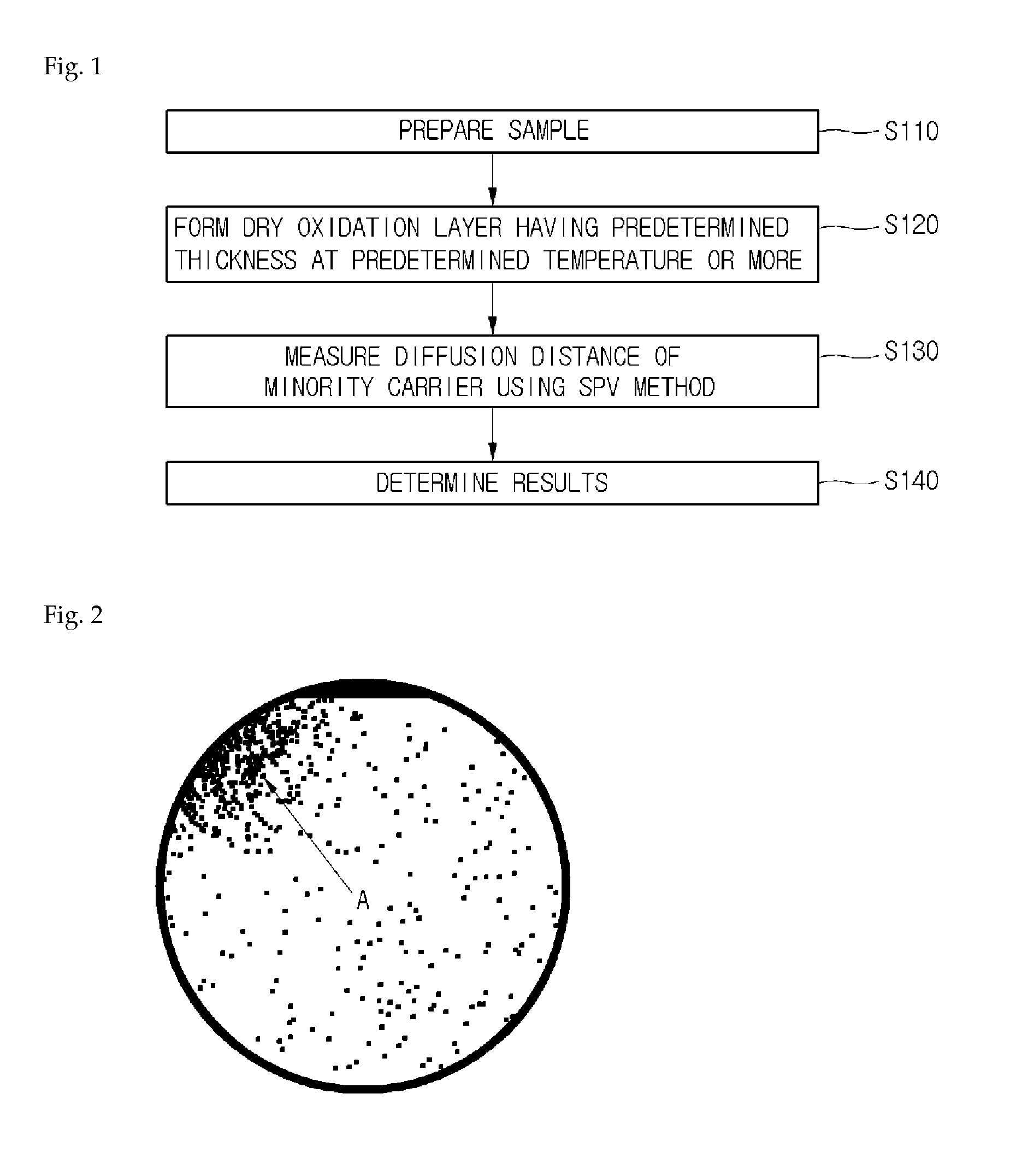
Method for evaluating wafer defects
a technology of defect evaluation and wafer, applied in the direction of after-treatment details, semiconductor/solid-state device testing/measurement, instruments, etc., can solve the problems of oisfs, affecting the yield and quality of devices, and taking a long time to perform the above-described method
- Summary
- Abstract
- Description
- Claims
- Application Information
AI Technical Summary
Benefits of technology
Problems solved by technology
Method used
Image

Examples
embodiment 1
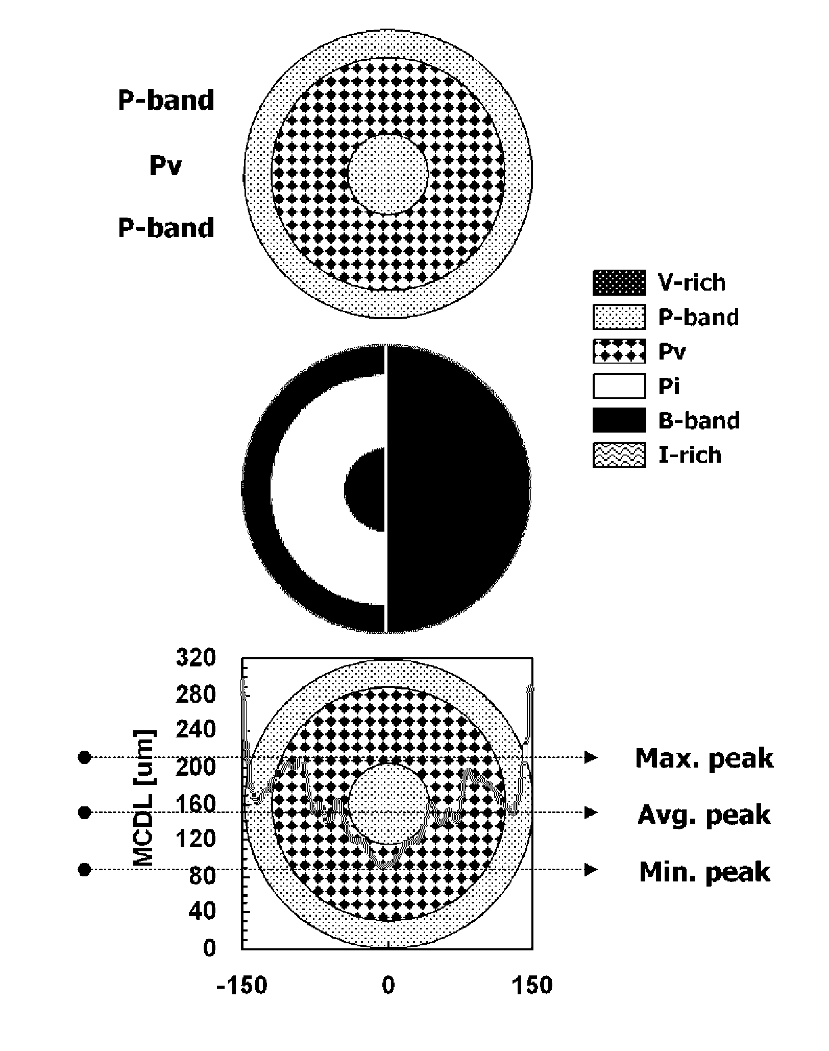
[0057]FIGS. 5 and 6 are graphs illustrating examples of diffusion distances of minority carriers for each crystal zone in a sample observed through a method for classifying silicon defect zones using the method for evaluating the silicon wafer point defects.
[0058]After the oxidation layer is formed to perform the current embodiment under the same sample, it may be seen that the zones are independently classified into the same zone as those of the existing methods in the evaluation results (a MCDL map) using the SPV method.
[0059]According to the results, although the evaluation results are obtained using the V-test in which an loop dominant point (LDP) defect zone is not included, it may be seen that the zones may be classified on the V-test including an interstitial rich zone in which the LDP defects are detected.
[0060]In case of FIG. 5, when the diffusion distances of the minority carriers have a profile shape from the V-rich to the Pi zone (IDP zone), the lowest value exists at a ...
PUM
 Abstract
Description
Claims
Application Information