
Semiconductor memory device and operating method thereof

Active Publication Date: 2014-05-08
SK HYNIX INC
View PDF5 Cites 22 Cited by
  • Summary
  • Abstract
  • Description
  • Claims
  • Application Information

AI Technical Summary

Benefits of technology

The present invention optimizes the read voltage used in a read operation to prevent errors and reduce the read operation time. The semiconductor memory device and its operating method change the read voltage through a moving read operation, a randomize operation, and a program / erase compensation operation. This ensures stable performance of the read operation and prevents errors even when there is a change in distribution of threshold voltages of the memory cells due to program / erase cycling or retention effect.

Problems solved by technology

However, according to the repeat of a program / erase operation in the memory cell, the electrons which have flowed in the floating gate are trapped in a tunnel oxidation layer, and the like.
However, as the size of the cell is decreased and the number of electrons stored in one cell is decreased, loss of one electron exerts large influence on the distribution.
Accordingly, there is a problem in that a left cell of a reference distribution (N+1) crosses a right cell of a directly lower distribution (N) of the reference distribution in the distribution.

Method used


Image

  • Semiconductor memory device and operating method thereof
  • Semiconductor memory device and operating method thereof
  • Semiconductor memory device and operating method thereof

Examples


Embodiment Construction

[0033]Hereinafter, an embodiment of the present invention will be described with reference to the accompanying drawings in detail.

[0034]However, the present invention is not limited to an embodiment disclosed below and may be implemented in various forms and the scope of the present invention is not limited to the following embodiments. Rather, the embodiments are provided to more sincerely and fully disclose the present invention and to completely transfer the spirit of the present invention to those skilled in the art to which the present invention pertains, and the scope of the present invention should be understood by the claims of the present invention.

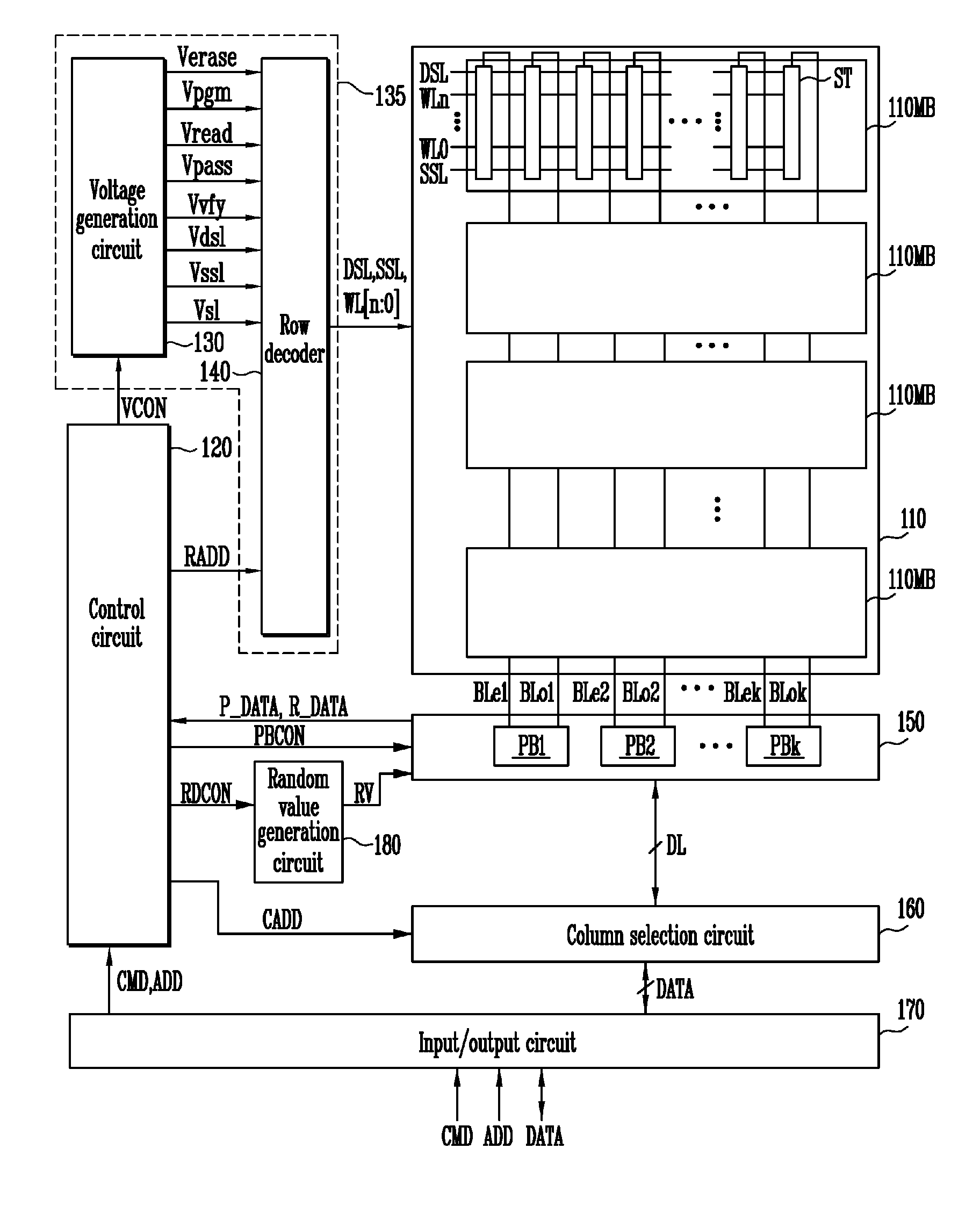
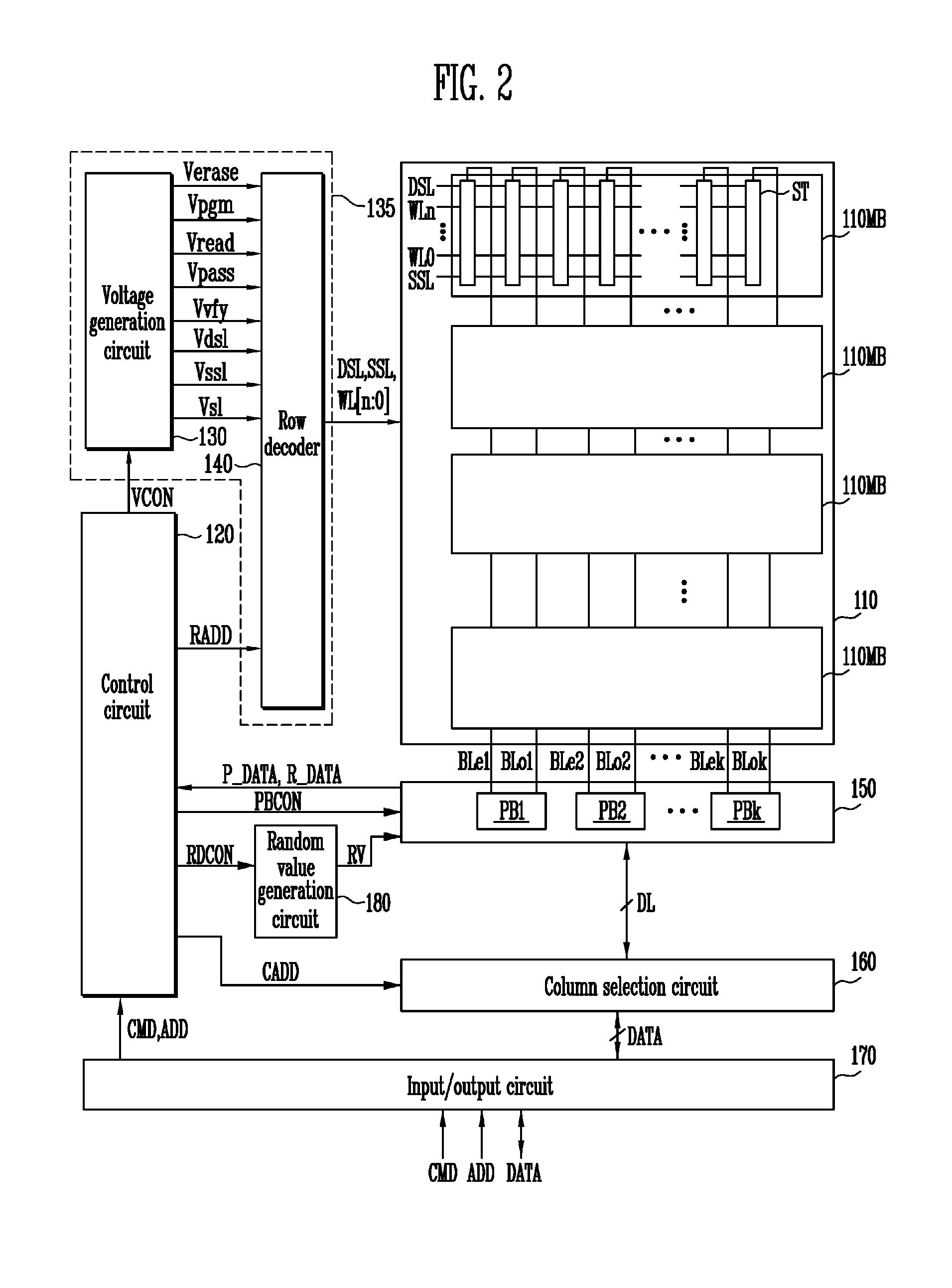
[0035]FIG. 2 is a block diagram illustrating a semiconductor memory device according to an embodiment of the present invention. FIG. 3 is a circuit diagram illustrating a memory block illustrated in FIG. 2.

[0036]The semiconductor memory device according to the embodiments of the present invention may include a memory array 110 in...


PUM


Abstract

A semiconductor memory device and an operating method of the semiconductor memory device change a read voltage used in a read operation by performing a moving read operation, a randomize operation, and a program / erase compensation operation independently or in combination, thereby stably performing the read operation without an error and reducing a time for the read operation even when distribution of threshold voltages of the memory cells is changed according to a program / erase cycling effect or a retention effect.

Description

CROSS-REFERENCE TO RELATED APPLICATION[0001]This application is based on and claims priority from Korean Patent Application No. 10-2012-0124234, filed on Nov. 5, 2012, with the Korean Intellectual Property Office, the disclosure of which is incorporated herein in its entirety by reference.BACKGROUND[0002]1. Technical Field[0003]The present invention generally relates to a semiconductor memory device performing a read operation and an operating method thereof.[0004]2. Related Art[0005]FIG. 1 is a graph for describing a change in distribution of threshold voltages of memory cells by cycling and retention effects.[0006]In general, in order to store data in memory cells of a semiconductor memory device, a threshold voltage of the memory cell is increased by performing a program operation. When a high voltage is applied to a control gate in the program operation, electrons flow in a floating gate by FN tunneling to increase the threshold voltage of the memory cell. However, according to ...

Claims


Application Information

Patent Timeline
IPC IPC(8): G11C16/26G11C16/10
CPCG11C16/10G11C16/26G11C11/5628G11C11/5635G11C11/5642G11C16/0483G11C16/3427G11C16/349G11C2216/14G11C16/34
Inventor KANG, WON KYUNG
Owner SK HYNIX INC
Features
  • Generate Ideas
  • Intellectual Property
  • Life Sciences
  • Materials
  • Tech Scout
  • Unparalleled Data Quality
  • Higher Quality Content
  • 60% Fewer Hallucinations
Learn More