High frequency circuit module

a high frequency circuit and module technology, applied in the direction of high frequency circuit adaptation, cross-talk/noise/interference reduction, printed circuit non-printed electric component association, etc., can solve the problem of difficult to achieve sufficient embedding a high frequency switch, and inability to further size reduction and thickness reduction. , to achieve the effect of preventing characteristic degradation and size reduction

Active Publication Date: 2014-05-15
TAIYO YUDEN KK
View PDF8 Cites 22 Cited by
  • Summary
  • Abstract
  • Description
  • Claims
  • Application Information

AI Technical Summary

Benefits of technology

[0022]As described above, with the multilayer circuit substrate of the present invention, it is possib

Problems solved by technology

However, with conventional configurations of a high frequency circuit module, due to a problem of characteristics degradation caused by interference between signal lines or a stray capacitance between a signal line and a ground pattern, the further size reduction and thickness reduction were not possible.
However, in the configurations disclosed in Patent Documents 1 to 3 above, it was difficult to achieve sufficient size reduction and thickness reduction by merely embedding a high frequency switch in a circuit substrate.
Also, in the configuration of Patent Document 1 above, ground wiring PG is disposed under the high frequency switch IC, but when the high frequency switch IC and the ground wiring are too close, the characteristic degradation would occur due to a stray capacitance between the two.
In the configuration disclosed in Patent Document 2 above, a ground electrode 12 is disposed directly below a pad for mounting a GaAs switch el

Method used


Image

  • High frequency circuit module
  • High frequency circuit module
  • High frequency circuit module

Examples


Embodiment Construction

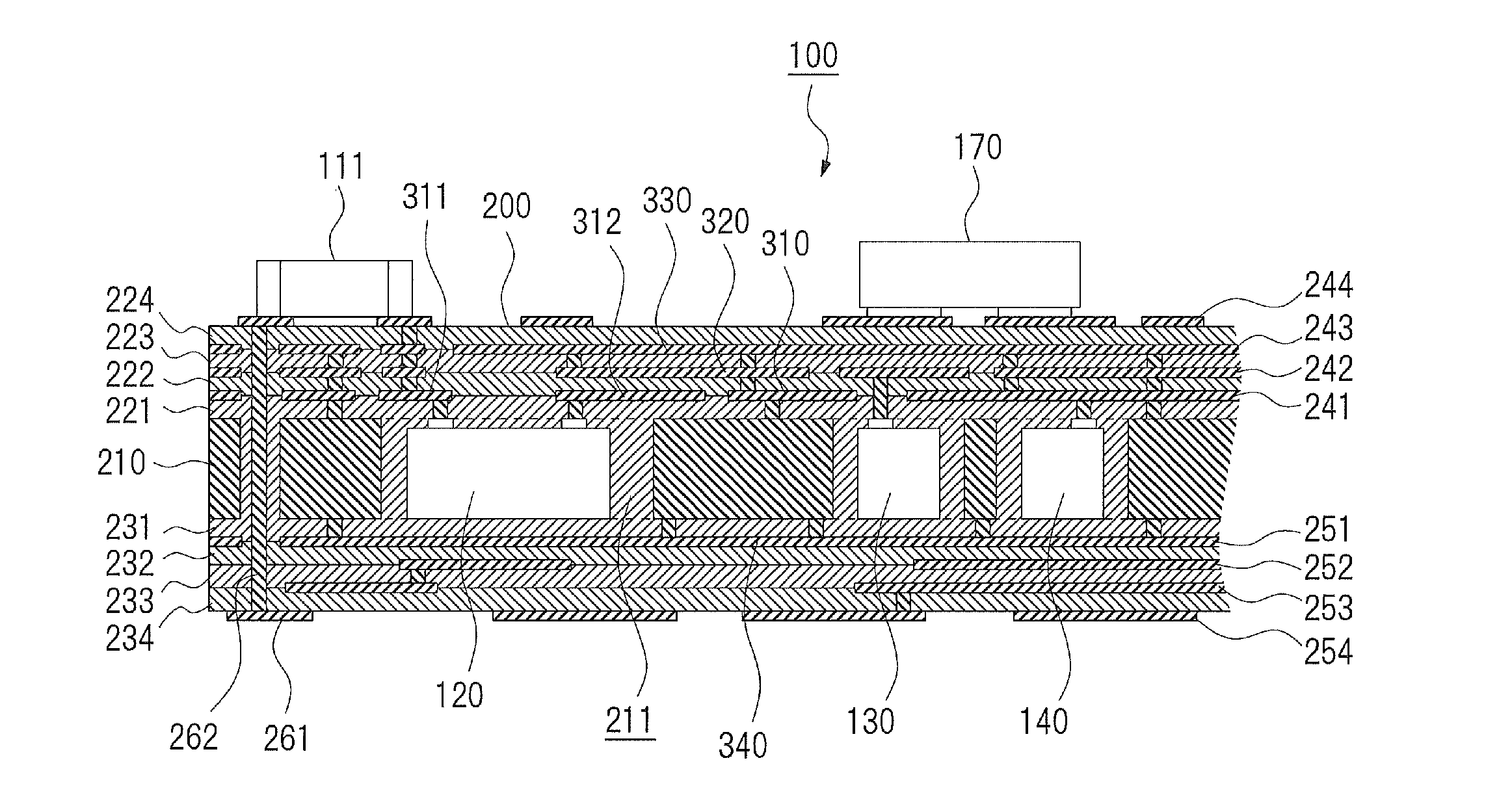
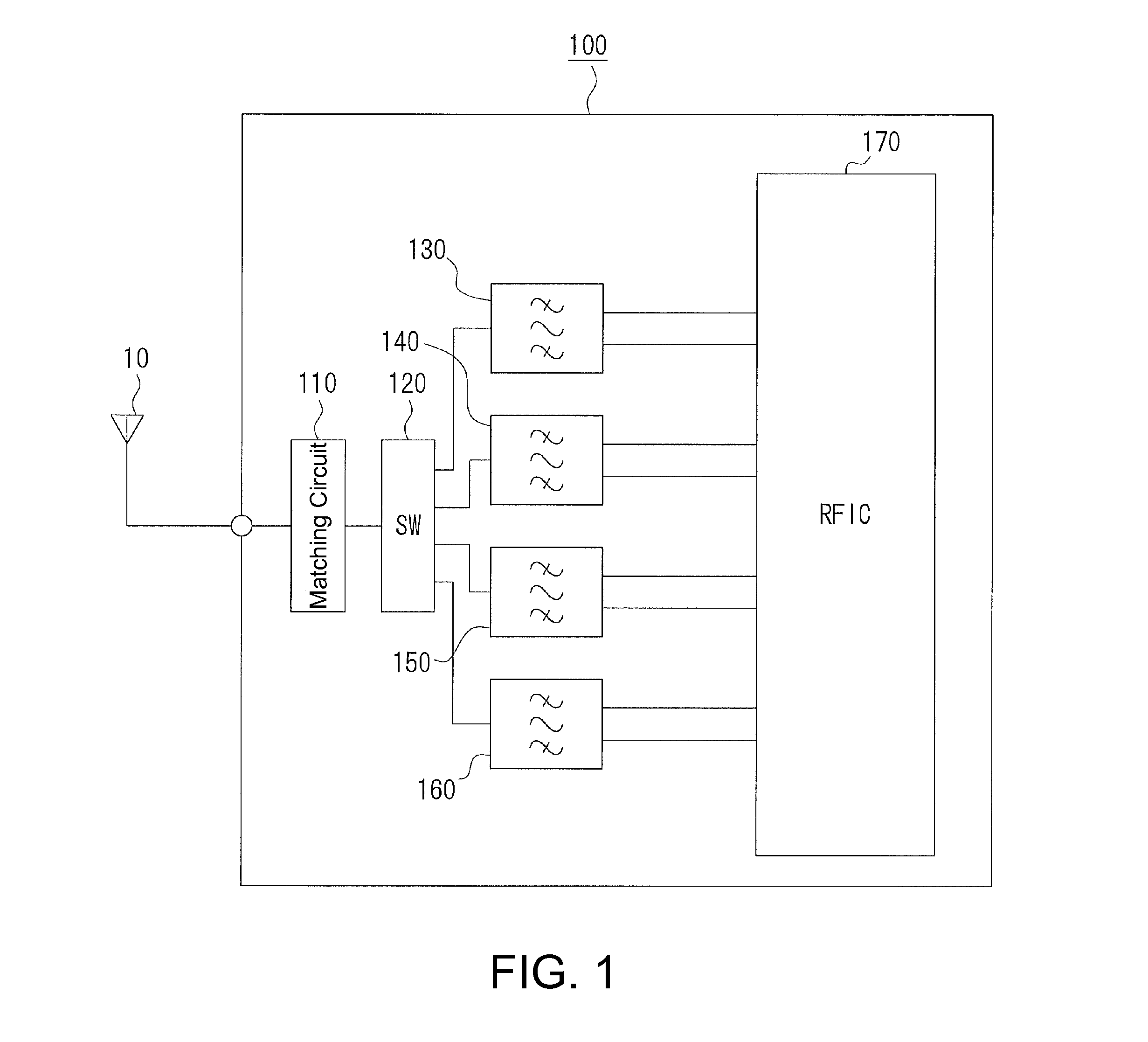
[0027]A high frequency circuit module according to Embodiment 1 of the present invention will be explained with reference to figures. FIG. 1 is a schematic circuit diagram of the high frequency circuit module. In the present embodiment, for ease of explanation, main configurations relating to the gist of the present invention will be explained.

[0028]A high frequency circuit module 100 of the present embodiment is used for a mobile phone that handles four frequency bands. The high frequency circuit module 100 has a diversity configuration, and includes a pair of transmission / reception circuits for one antenna, and one reception circuit for another antenna. In the present embodiment, the reception circuit of the latter will be explained.

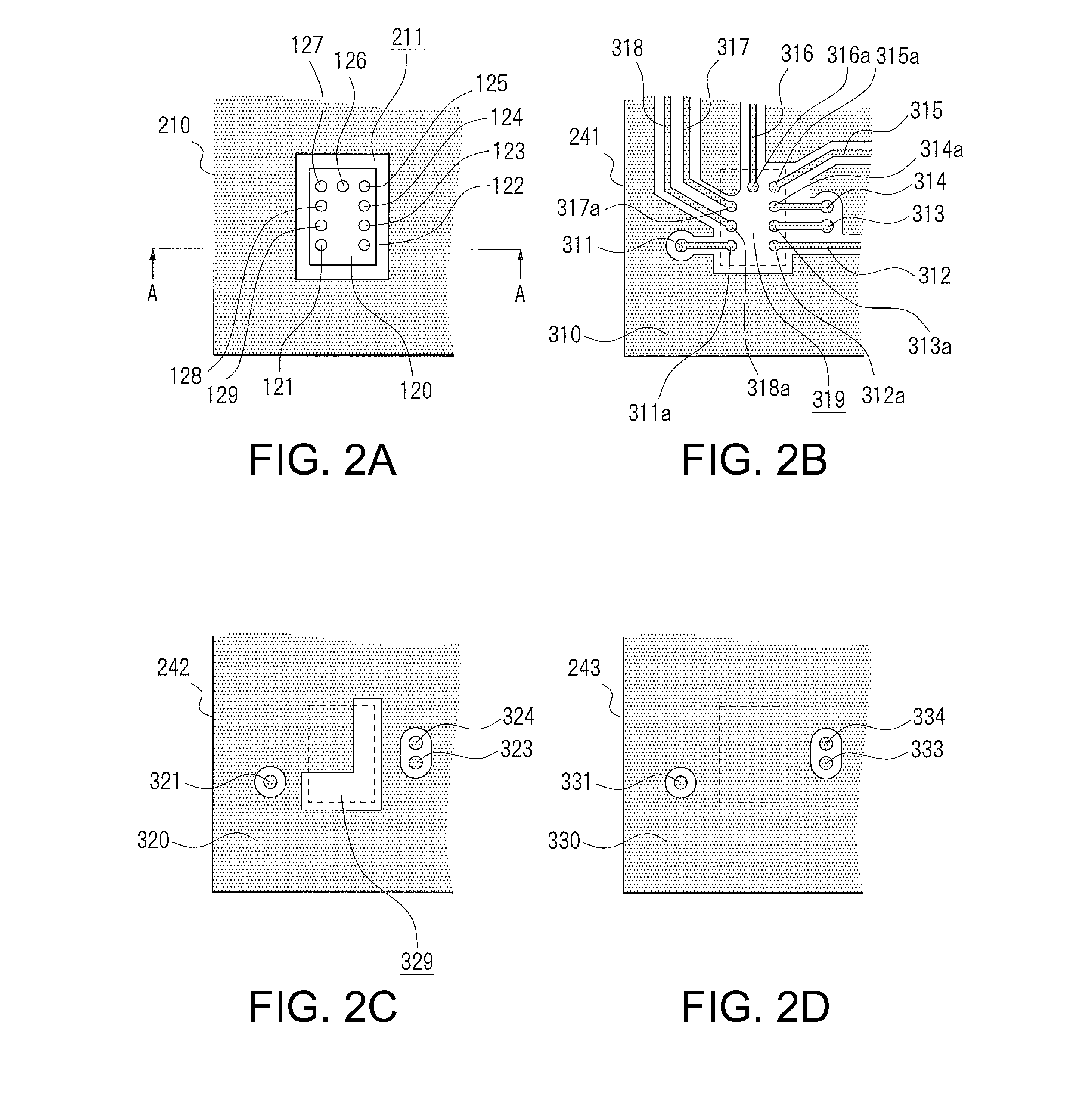
[0029]As shown in FIG. 1, the high frequency circuit module 100 includes a matching circuit 110 to eliminate a mismatch with the antenna, a high frequency switch 120 that switches connections of the antenna for the respective frequency bands, first to ...


PUM


Abstract

A multilayer circuit substrate has a high frequency switch embedded therein. In the multilayer circuit substrate, a first conductive layer that faces a main surface of the high frequency switch through an insulating layer has circuit patterns formed therein so as to be connected to input/output terminals through via conductors. The first conductive layer has an opening pattern in which a ground conductor is not present in a region that faces the main surface of the high frequency switch and that is outside of the circuit patterns. In a third conductive layer disposed outer side of the first conductive layer with respect to the high frequency switch, a ground conductor is formed at least in a region where the main surface of the high frequency switch is projected in the thickness direction.

Description

[0001]This application claims the benefit of Japanese Application No. 2012-248255, filed in Japan on Nov. 12, 2012, which is hereby incorporated by reference in its entirety.BACKGROUND OF THE INVENTION[0002]1. Field of the Invention[0003]The present invention relates to a high frequency circuit module in which a high frequency circuit is mounted on a multilayer circuit substrate, and more particularly, to an installation structure of a high frequency switch that switches connection between an antenna and a high frequency circuit.[0004]2. Description of Related Art[0005]Conventionally, in circuit modules including high frequency switches used for mobile phones, switching circuits utilizing PIN diodes have been employed. However, with a recent trend for capabilities of handling multiple bands and higher communication frequency band, high frequency switches utilizing FET switches have been more widely used. Known examples of circuit modules with this type of high frequency switches inc...

Claims


Application Information

Patent Timeline
IPC IPC(8): H05K1/02
CPCH05K1/0237H01L24/19H01L2223/6677H01L2224/04105H01L2224/16225H01L2224/73267H01L2924/19105H05K1/0233H05K1/0243H05K1/0253H05K1/185H01L24/24
Inventor SAJI, TETSUONAKAMURA, HIROSHI
Owner TAIYO YUDEN KK
Why Eureka
Try Eureka