Nanowire Sized Opto-Electronic Structure and Method for Modifying Selected Portions of Same

a technology of opto-electronic structure and nanowire, which is applied in the field of nanostructures, can solve the problems that the shape of nanostructures can have challenges in device design, and achieve the effects of high mg/ga, and reducing or eliminating the conductivity of the tips

Active Publication Date: 2014-05-22
NANOSYS INC
View PDF9 Cites 31 Cited by
  • Summary
  • Abstract
  • Description
  • Claims
  • Application Information

AI Technical Summary

Benefits of technology

[0005]In certain embodiments, the invention provides a method for making a LED structure that comprises a support and a plurality of nanowires arrayed on the support, wherein each nanowire comprises a tip and a sidewall, wherein the method comprises reducing or eliminating the conductivity of the tips of the nanowires compared to the conductivity of the sidewalls during or after creation of the nanowires. In certain of these embodiments, conditions during or after creation of the nanowires are controlled such that the conductivity of the tips is reduced by at least one order of magnitude compared to the conductivity of the tips without the controlling of the conditions. In certain embodiments, the controlling of the conditions comprises forming an insulating layer after the creation of the nanowires. In certain embodiments, the insulating layer is formed over the array of nanowires so that insulation is layered on the tips and the sidewalls, then the array is subjected to etching under conditions that removes the insulating layer on the sidewalls but that leaves at least part of the insulating layer on the tips. In certain embodiments, the insulating layer comprises SiOx, such as SiO2. In certain embodiments, the condition that removes the insulating layer on sidewalls but leaves at least part on the tips comprises etching, such as anisotropic etching. In certain embodiments, the nanowires comprise a first conductivity type core and a second conductivity type shell, and the sidewalls and tips comprise the second conductivity type shell. In some of these embodiments, the shell is formed in successive layers such as successive layers of lower conductivity material and higher conductivity material, wherein the higher conductivity material preferentially forms on the sidewalls compared to the tips. In certain of these embodiments, the lower conductivity material comprises p-AlGaN and the higher conductivity material comprises p-GaN. In certain embodiments the shell is formed to provide a plurality of the lower conductivity layers and a plurality of the higher conductivity layers on the sidewalls. In some of these embodiments, the shell is formed to provide only a single lower conductivity layer on the tips. In other embodiments, the shell is formed to provide a plurality of the lower conductivity layers and a plurality of the higher conductivity layers on the tips, wherein the thickness of the higher conductivity layers on the tips is less than that on the sidewalls, such that the tips are less conductive than the sidewalls, such as nonconductive. In certain embodiments where a core and shell are constructed, the method comprises forming a highly resistive material on the tips but not on the sidewalls of the nanowires. In some of these embodiments, the highly resistive material is formed on the tips after the shell is completed. In other of these embodiments, the highly resistive material is formed on the tips before the shell is completed. In certain embodiments, the highly resistive material comprises pGaN that comprises a very high Mg / Ga ratio and a low V / III ratio. In certain embodiments where a core and a shell are constructed, at least one layer of the shell is formed in a carrier gas that comprises H2, such as a carrier gas that comprises at least 50 sccm H2. In certain embodiments, where the nanowires include a core and a shell, the first conductivity type semiconductor nanowire core is enclosed by the second conductivity type semiconductor shell for forming a pn or pin junction that in operation provides an active region for light generation. The first conductivity type may comprise n-type, and the second conductivity type may comprise p-type. In certain embodiments, a support comprises a n-type buffer layer from which the nanowire core is grown during production of the array of nanowires. In certain embodiments, the support further comprises a dielectric masking layer, such that cores protrude from the buffer layer through openings in the masking layer, and the shells are located on the masking layer. In certain embodiments, the support further comprises a substrate layer beneath the buffer layer. In certain embodiments, the substrate layer comprises Al2O3. In certain embodiments, the support layer further comprises a reflective layer, such as Ag.

Problems solved by technology

The three-dimensional shape of the nanostructures can have challenges in device design.

Method used


Image

  • Nanowire Sized Opto-Electronic Structure and Method for Modifying Selected Portions of Same
  • Nanowire Sized Opto-Electronic Structure and Method for Modifying Selected Portions of Same
  • Nanowire Sized Opto-Electronic Structure and Method for Modifying Selected Portions of Same

Examples


Embodiment Construction

[0023]The invention provides methods for altering the properties of selected areas of nanowire based structures, in particular opto-electronic structures such as LEDs, for example, nanowire light emitting diodes (LEDs), e.g., altering the properties to decrease conductivity of selected portions of nanowires in a nanowire LED. The invention also provides compositions that can be fabricated, e.g., using the methods of the invention.

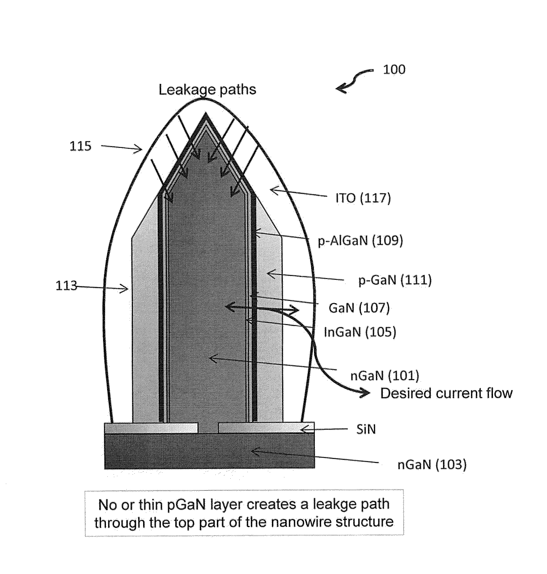
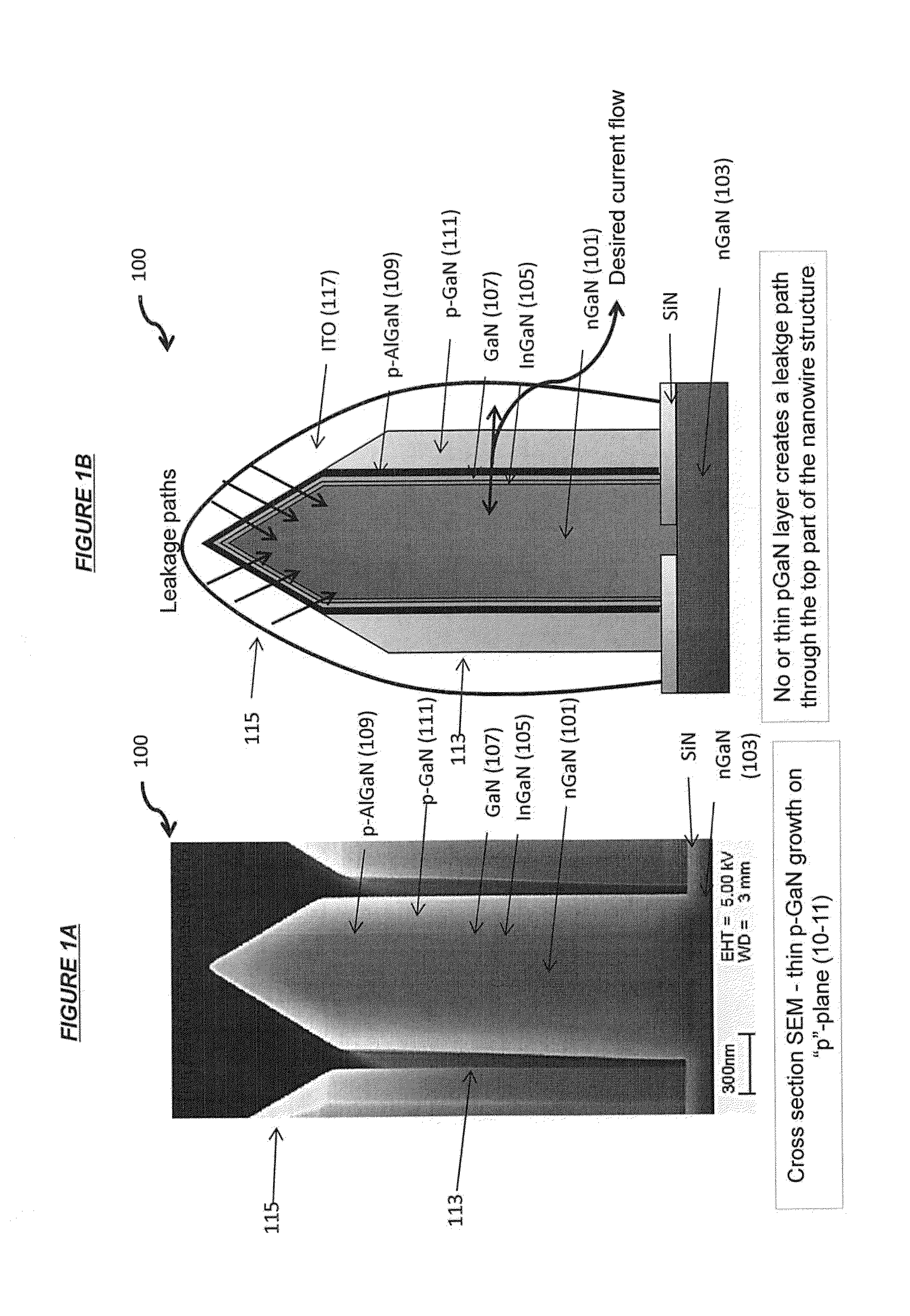
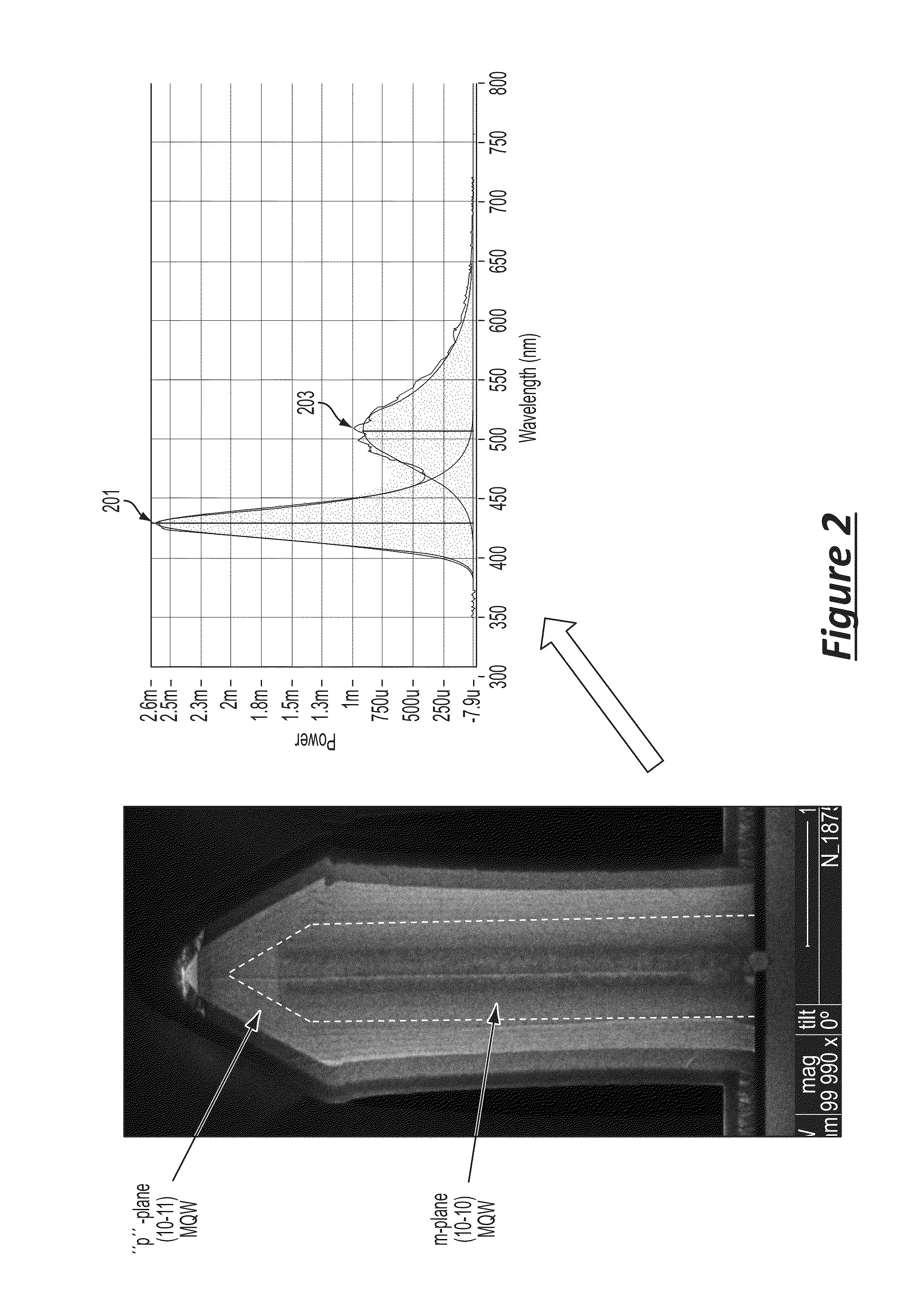
[0024]The 3-dimensional nature of LEDs made from nanowires emerging from a planar surface can present challenges in device design. Different crystallographic planes can give different growth rates, material composition, and doping. This can, for example, cause leakage paths and multiple emission wavelengths not desirable for the device. An example is a nanowire LED as illustrated in FIG. 1. In this example, a nanowire LED 100 includes a n-GaN core 101 in electrical contact with an n-GaN buffer layer 103, intermediate layers of InGaN 105, GaN 107, and p-AlGa...


PUM

PropertyMeasurementUnit
thickaaaaaaaaaa
thickaaaaaaaaaa
current leakageaaaaaaaaaa

Abstract

A LED structure includes a support and a plurality of nanowires located on the support, where each nanowire includes a tip and a sidewall. A method of making the LED structure includes reducing or eliminating the conductivity of the tips of the nanowires compared to the conductivity of the sidewalls during or after creation of the nanowires.

Description

RELATED APPLICATION[0001]This application claims the benefit of priority to U.S. Provisional Application Ser. No. 61 / 719,133, filed on Oct. 26, 2012, the entire contents of which are incorporated herein by reference.FIELD[0002]The present invention is directed generally to nanostructures and method of making thereof and specifically to nanowire LEDs and methods of making thereof.BACKGROUND OF THE INVENTION[0003]Nanostructures are promising building blocks for electronic and optoelectronic semiconductor devices. The three-dimensional shape of the nanostructures can have challenges in device design. Different crystallographic planes can give different growth rate, material composition, and doping.SUMMARY OF THE INVENTION[0004]In one aspect, the invention provides methods.[0005]In certain embodiments, the invention provides a method for making a LED structure that comprises a support and a plurality of nanowires arrayed on the support, wherein each nanowire comprises a tip and a sidewa...

Claims


Application Information

Patent Timeline
Patent Type & Authority Applications(United States)
IPC IPC(8): H01L33/24H01L33/06
CPCH01L33/24H01L33/06B82Y20/00H01L33/007H01L33/08H01L33/16H01L21/0237H01L21/02439H01L21/02458H01L21/02505H01L21/02513H01L21/02521H01L21/0254H01L21/02603H01L21/02639H01L33/0075H01L33/44H01L2933/0025
Inventor SVENSSON, CARL PATRIK THEODORGARDNER, NATHAN
Owner NANOSYS INC
Why Eureka
Try Eureka