Iii-nitride device with back-gate and field plate and process for its manufacture

Inactive Publication Date: 2010-03-18
INTERNATIONAL RECTIFIER COEP
View PDF11 Cites 86 Cited by
  • Summary
  • Abstract
  • Description
  • Claims
  • Application Information

AI Technical Summary

Benefits of technology

[0008]The back-gate can be connected to the main gate or can have a separate terminal. The application of a negative voltage to the back-gate reduces the conductivity in the leakage paths in the GaN layer and also improves the subthreshold characteristics. The transconductance of the device is also improved, since the back-gate introduces 2DEG channel control from the backside. The back-gate size may be varied to achieve optimal subthreshold and tran

Problems solved by technology

However, leakage paths exist in the GaN layer which is normally relatively highly doped.
The device a

Method used


Image

  • Iii-nitride device with back-gate and field plate and process for its manufacture
  • Iii-nitride device with back-gate and field plate and process for its manufacture
  • Iii-nitride device with back-gate and field plate and process for its manufacture

Examples


first embodiment

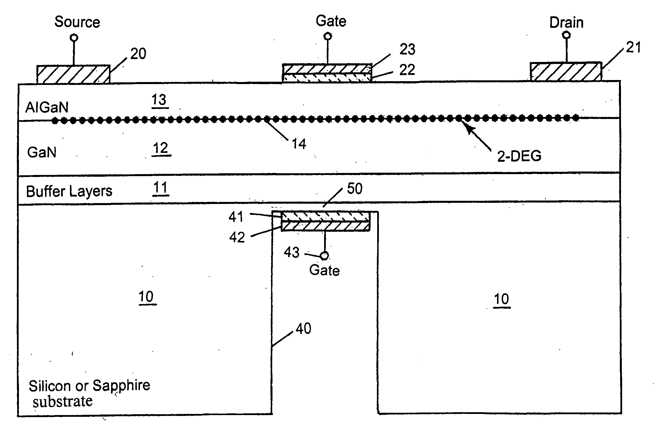
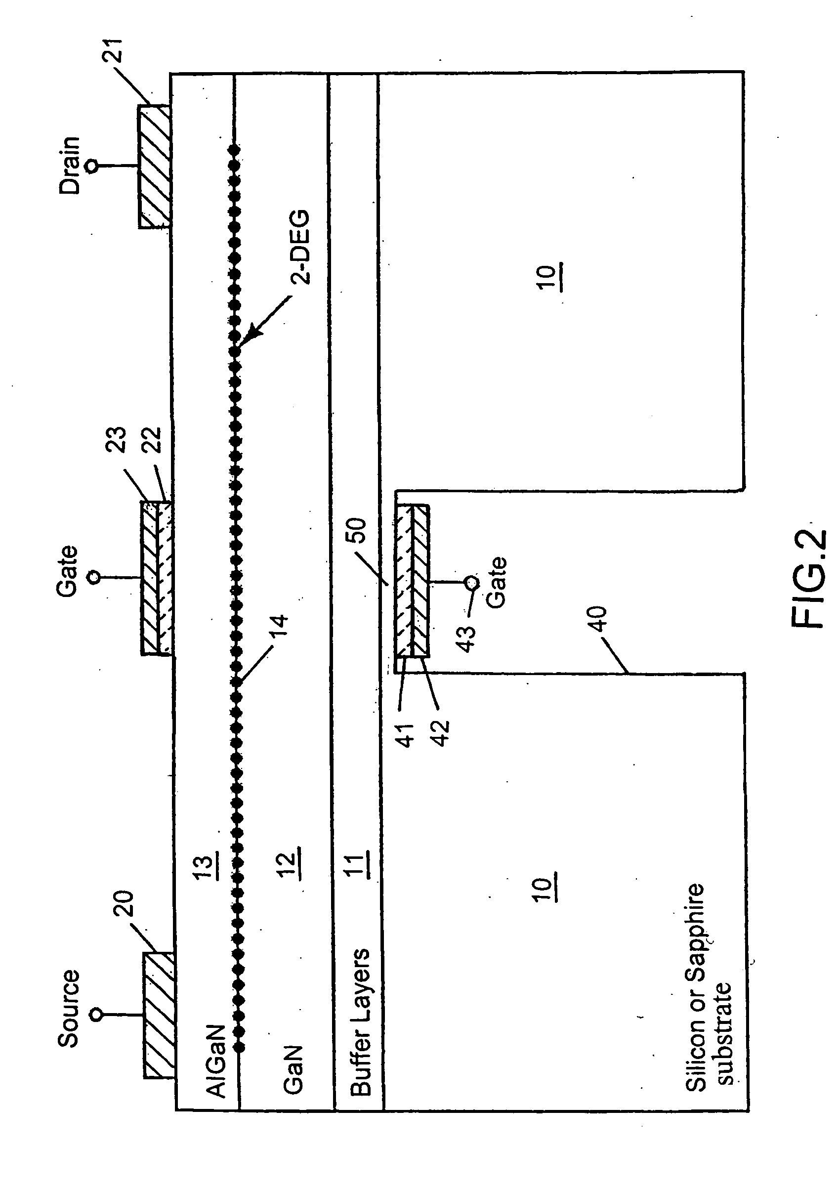
[0023]FIG. 2 shows the invention in which a back-side trench or etch 40 is formed in the back or bottom of substrate 10. A gate dielectric 41 is formed and patterned at the bottom of trench 40 and adjacent the buffer layers 11. A conductive back-gate or secondary gate 42 is then deposited on dielectric 41 and is suitably patterned. Back-gate 42 is laterally aligned with and is under gate 23.

[0024]Back-gate 42 can be connected to main gate 23 or can have its own terminal 43 as shown which is connected to gate potential or any potential desired. The application of a negative voltage to back-gate 42 reduces leakage paths in GaN layer 12 between source and drain 20 and 21 respectively and also improves the sub threshold characteristics. The transconductance of the device also improves since the back-gate 42 introduces 2 DEG channel 14 control from the back-side of the device.

[0025]In a typical device, a silicon substrate 10 having a thickness of 600 μm and resistivity of 10 ohm cm can b...

second embodiment

[0027]FIG. 3 shows the invention in which the trench 40 (formed by any well know technique) is deeper than in FIG. 2 and extends into buffer layers 11 by about 0.5 μm. This places the back-gate 42 closer to the 2 DEG layer 14. The closer placement of gate 42 to 2 DEG layer 14 allows further improvements such as even less leakage and better transconductance and subthreshold slope.

[0028]FIG. 4 shows a further embodiment of the invention in which a field plate is added to the embodiment of FIG. 2. Thus, in FIG. 4, a second trench 60 is etched into substrate 10 and under the drift region in GaN layer 12 between the gate 23 and drain 21. Trench 60 receives a dielectric layer 61 and conductive field plate 62 which are coplanar with dielectric 41 and back-gate 42 and may have the same thicknesses and are deposited and patterned in the same deposition and etch steps. Field plate 62 has a terminal 63 which may be connected to source electrode 20.

[0029]By applying an appropriate bias to field...


PUM


Abstract

A III-Nitride device has a back-gate disposed in a trench and under and in close proximity to the 2 DEG layer and in lateral alignment with the main gate of the device. A laterally disposed trench is also disposed in a trench and under and in close proximity to the drift region between the gate and drain electrodes of the device. The back-gate is connected to the main gate and the field plate is connected to the source electrode. The back-gate can consist of a highly conductive silicon substrate.

Description

FIELD OF THE INVENTION[0001]This invention relates to III-Nitride devices and processes for their manufacture and more specifically relates to the improvement of the leakage, subthreshold leakage and transconductance characteristics of such devices.BACKGROUND OF THE INVENTION[0002]III-Nitride devices are normally-on depletion mode (D-mode) devices. A negative voltage is applied to the gate of the device to turn it off In a typical III-Nitride device, an AlGaN layer atop a GaN layer forms a 2DEG, normally conductive layer which conducts under a control gate and between a source and a drain electrode atop and in contact with the AlGaN layer.[0003]However, leakage paths exist in the GaN layer which is normally relatively highly doped. The device also suffers from sub-threshold characteristics and relatively poor transconductance characteristics.[0004]It would be desirable to provide a III-Nitride device which improves the leakage, the subthreshold characteristics and transconductance o...

Claims


Application Information

Patent Timeline
IPC IPC(8): H01L47/00
CPCH01L29/2003H01L29/7787H01L29/42356H01L29/407H01L29/205H01L29/7831H01L29/7832H01L29/8124
Inventor CHARLES, ALAINBAHRAMIAN, HAMID TONY
Owner INTERNATIONAL RECTIFIER COEP
Why Eureka
Try Eureka