Blue phosphorescence compound and organic light emitting diode using the same

Active Publication Date: 2014-05-22
LG DISPLAY CO LTD
View PDF2 Cites 3 Cited by
  • Summary
  • Abstract
  • Description
  • Claims
  • Application Information

AI Technical Summary

Benefits of technology

The patent describes an organic light emitting diode (OLED) that uses a blue phosphorescence compound with high efficiency and high triplet energy as the host of its light emitting layer. This compound has a symmetrical or asymmetrical substitution at certain positions in the dibenzofuran core and is made up of either an aromatic or heterocyclic compound. The technical effect of this innovation is that it has improved the efficiency of OLEDs, resulting in more efficient and effective light emitting devices.

Problems solved by technology

Hence, efficiency of the organic light emitting diode is sharply reduced.

Method used


Image

  • Blue phosphorescence compound and organic light emitting diode using the same
  • Blue phosphorescence compound and organic light emitting diode using the same
  • Blue phosphorescence compound and organic light emitting diode using the same

Examples


manufacturing example 1

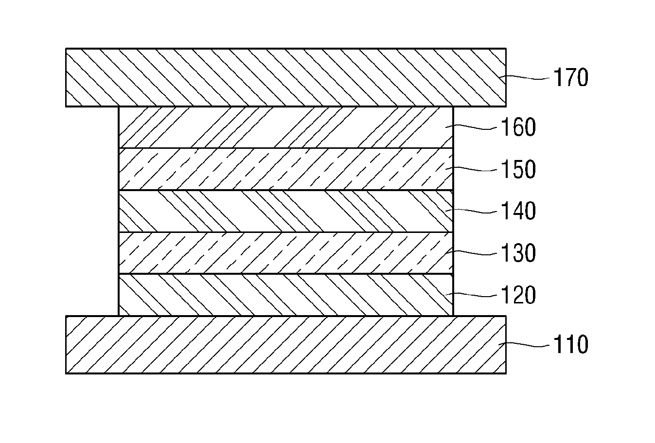
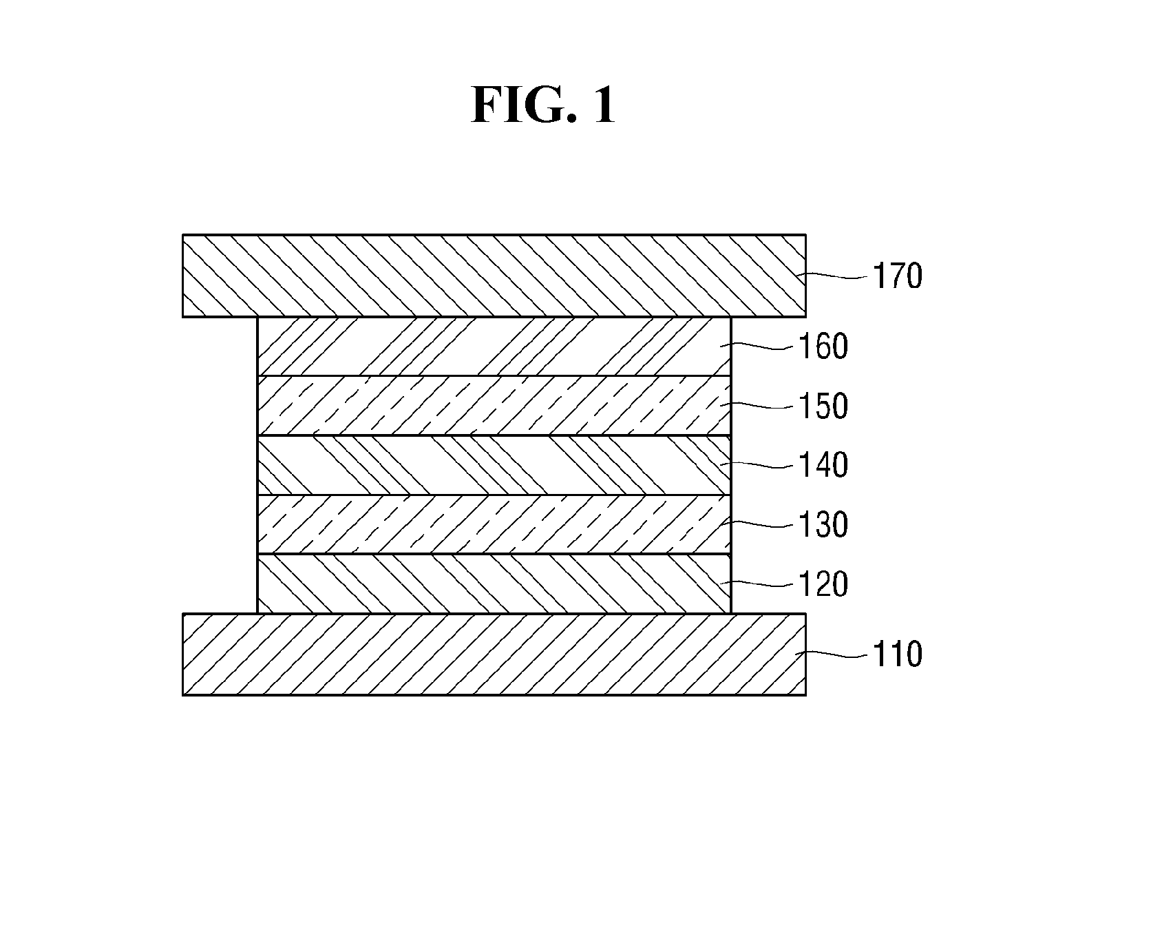
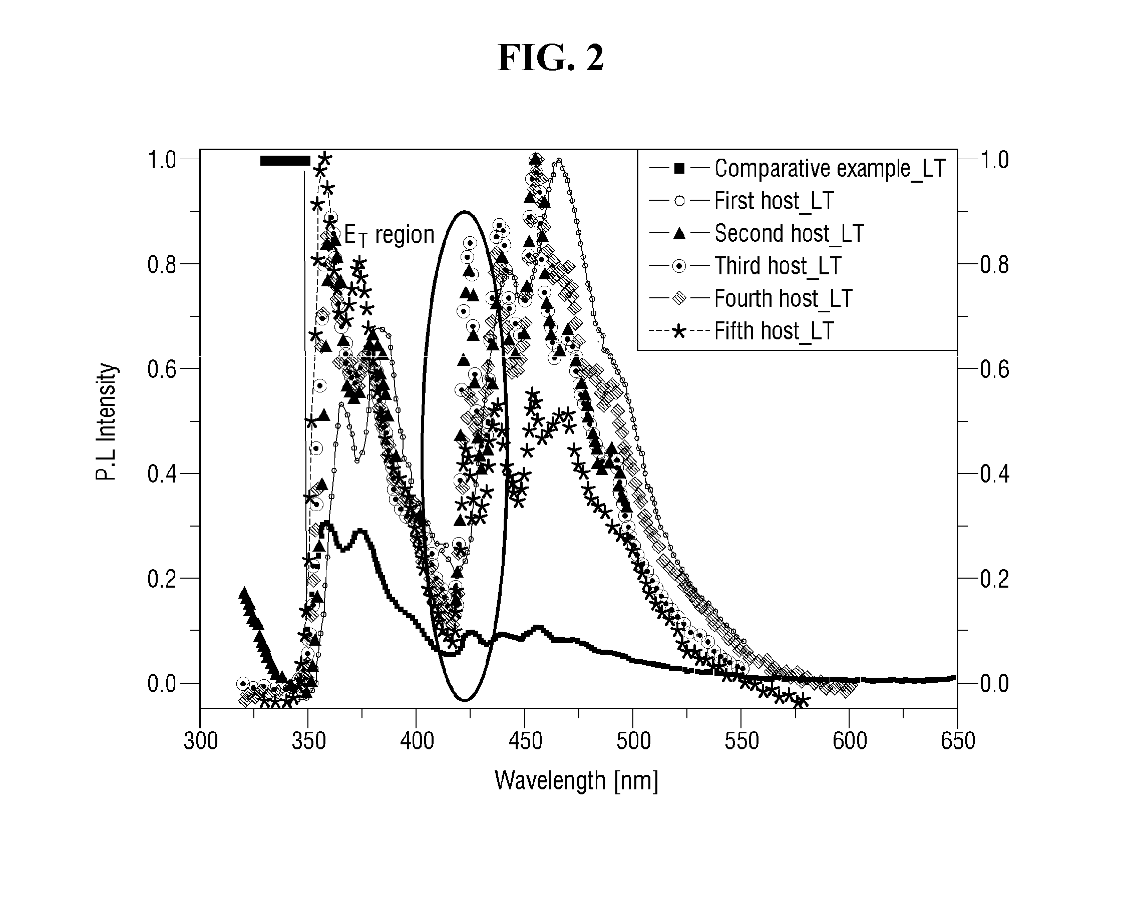
[0059]An ITO substrate was patterned to have a light emitting area of 3 mm×3 mm and then washed. After the ITO substrate was installed in a vacuum chamber, a base pressure was made to be 1×10⁻⁶ torr. Then, on ITO for forming an anode, HAT-CN for a hole injection layer was formed with a thickness of about 50 Å, NPD for a hole transport layer was formed with a thickness of about 550 Å, TAPC for an electron blocking layer was formed with a thickness of about 100 Å, and the second host material having a thickness of about 300 Å as a host and [FCNIr] having a doping concentration of about 15% as a dopant were formed for a light emitting layer. Then, TmPyPb for an electron transport layer was formed with a thickness of about 400 Å, LiF for an electron injection layer was formed with a thickness of about 5 Å, and Al for a cathode was formed with a thickness of about 1,100 Å. Then, an encapsulation process using UV curable epoxy and a moisture getter was performed, thereby manufacturing an ...

manufacturing example 2

[0060]An organic light emitting diode was manufactured under the same process conditions as the above manufacturing example 1, only except that the third host material was used as a host of a light emitting layer.


PUM


Abstract

A blue phosphorescence compound and an organic light emitting diode using the same are disclosed. The blue phosphorescence compound is represented by Chemical Formula 1 below:wherein ‘A’ and ‘B’ are symmetrically or asymmetrically substituted at positions of Nos. 2 and 7 or Nos. 3 and 6 of dibenzofuran core and are independently formed of an aromatic cyclic compound or a heterocyclic compound.

Description

[0001]This application claims the priority benefit of Korean Patent Application No. 10-2012-0132847 filed on Nov. 22, 2012, which is incorporated herein by reference for all purposes as if fully set forth herein.BACKGROUND OF THE INVENTION[0002]1. Field of the Invention[0003]Embodiments of the invention relate to a blue phosphorescence compound and an organic light emitting diode using the same, and more particularly, to an organic light emitting diode using a high efficiency blue phosphorescence compound having high triplet energy as a host of a light emitting layer.[0004]2. Discussion of the Related Art[0005]The importance of flat panel displays is recently increasing with the growth of multimedia. Thus, various types of flat panel displays such as a liquid crystal display (LCD), a plasma display panel (PDP), a field emission display (FED), and an organic light emitting display have been put to practical use to meet this trend.[0006]The organic light emitting display has advantage...

Claims


Application Information

Patent Timeline
IPC IPC(8): H01L51/00
CPCC07D405/14C07D471/04C07D519/00C09K11/06C09K2211/1029C09K2211/1088H10K85/6574H10K85/6572H10K50/11H10K2101/10C07D209/82
Inventor SONG, INBUMBAE, SUKYOUNG
Owner LG DISPLAY CO LTD
Why Eureka
Try Eureka