Power semiconductor module

a technology of semiconductor modules and solder junctions, applied in semiconductor devices, semiconductor/solid-state device details, electrical apparatus, etc., can solve the problems of cracks, cracks may be formed, and the solder junction region is the most vulnerable to cracks, so as to achieve the effect of long-term reliability and a considerable slowing of crack propagation in the solder junction region

Inactive Publication Date: 2014-05-22
SAMSUNG ELECTRO MECHANICS CO LTD
View PDF0 Cites 5 Cited by
  • Summary
  • Abstract
  • Description
  • Claims
  • Application Information

AI Technical Summary

Benefits of technology

[0022]The present invention has been made in an effort to provide a power semiconductor module in which a flux gas generated from a central portion of a substrate during a process of soldering a substrate and a base plate is easily discharged to the outside of the substrate, thus restraining a generation of a non-junction portion or a void, and a speed at which cracks propagate in a solder junction region is considerably slowed relative to the related art through structural stabilization, thus obtaining long-term reliability.

Problems solved by technology

In such a junction structure, the solder junction region between the substrate and the base plate is most vulnerable to crack.
Of course, the solder junction region is also vulnerable to crack.
First, during a soldering process, a solder flow on a smooth, uniform interface between the substrate and the base plate may sequentially proceed toward an outer side of the substrate along the plane, so a flux gas generated from a central portion of the substrate may not be discharged to the outer side of the substrate, generating a non-junction portion or a void.
Second, cracks may be formed in a solder junction region between the substrate and the base plate due to a difference between coefficients of thermal expansion of the substrate and the base plate according to a rapid change in temperature. In this case, the smooth, uniform interface between the substrate and the base plate causes cracks propagate faster, degrading long-term reliability of the power semiconductor module.

Method used


Image

  • Power semiconductor module
  • Power semiconductor module
  • Power semiconductor module

Examples


first embodiment

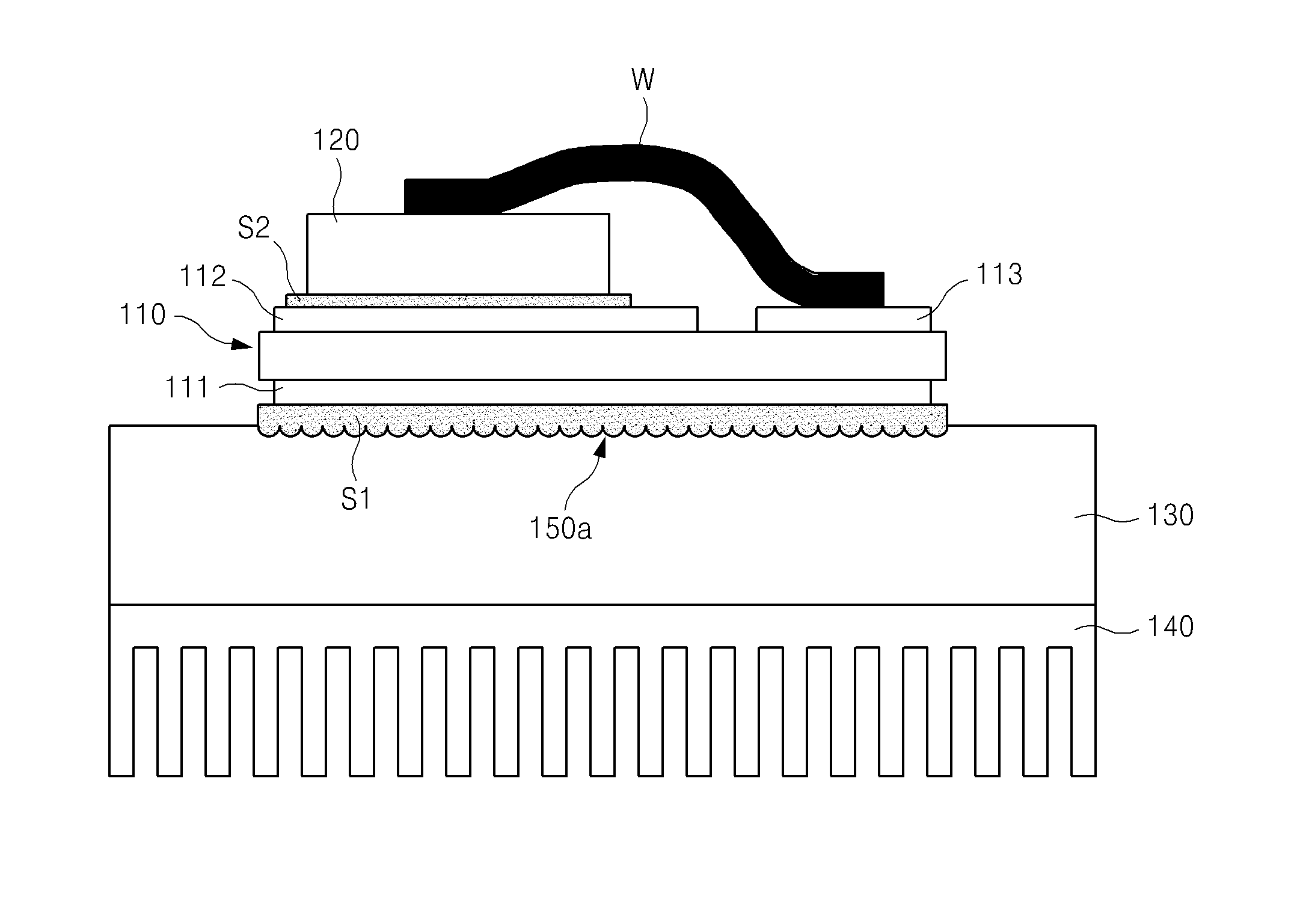
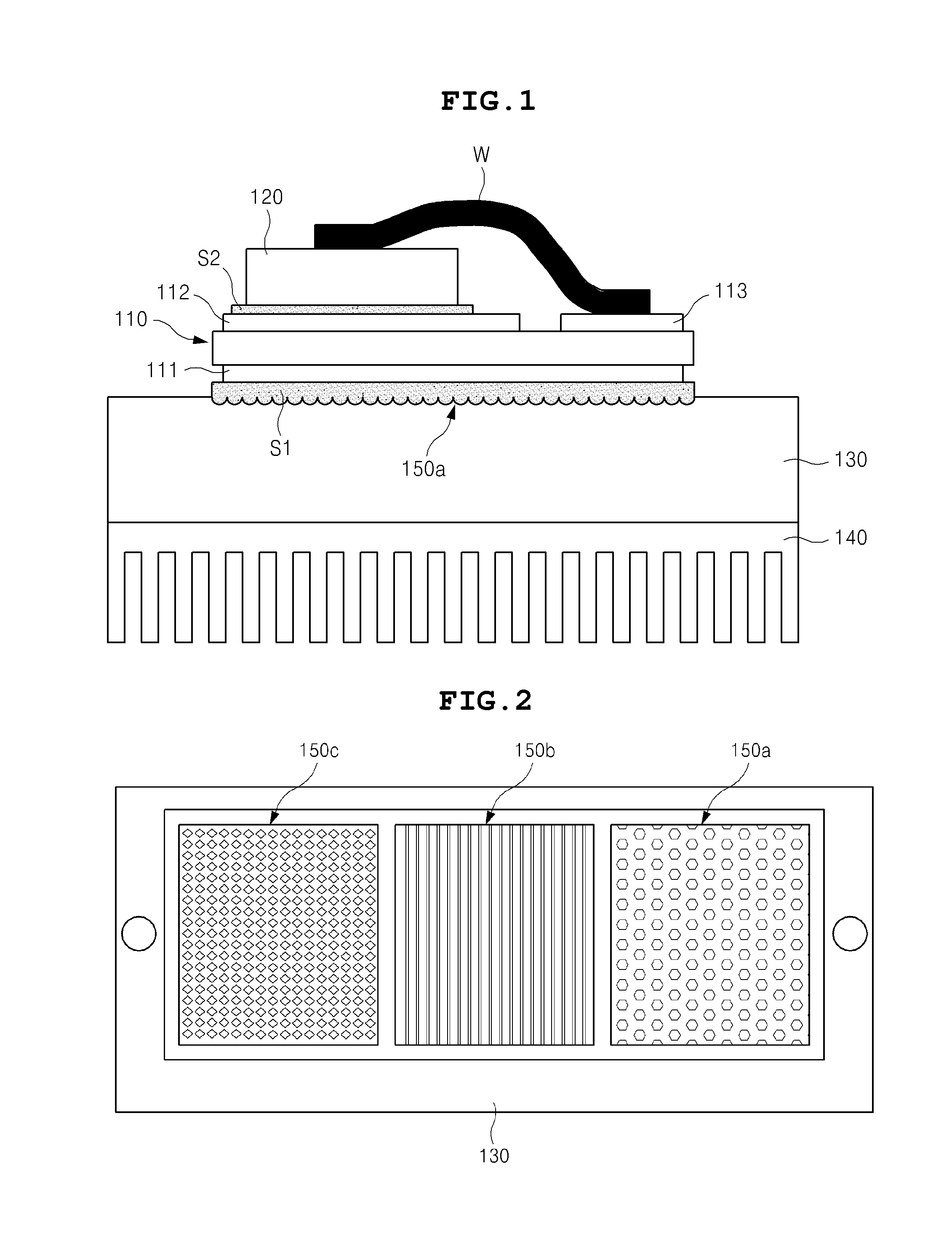
[0046]FIG. 1 is a view illustrating a power semiconductor module according to the present invention. FIG. 2 is a plan view of a base plate illustrated in FIG. 1. FIG. 3 is a view illustrating a lateral structure of FIG. 2.

[0047]Referring to FIGS. 1 to 3, a power semiconductor module according to the present embodiment aims at a high power application, having a structure in which a plurality of semiconductor elements 120 is mounted on a substrate 110. FIG. 1 illustrates a single semiconductor element 120, but it is merely an example and a plurality of semiconductor elements 120 may be formed on the substrate 110 to form the power semiconductor module.

[0048]In detail, the power semiconductor module according to an embodiment of the present invention includes the substrate 110 having a first metal conductive track 111 formed on one surface (i.e., a lower surface) thereof and a base plate 130 made of a metal and solder-joined with the substrate 110 in the metal conductive track 111 regi...

second embodiment

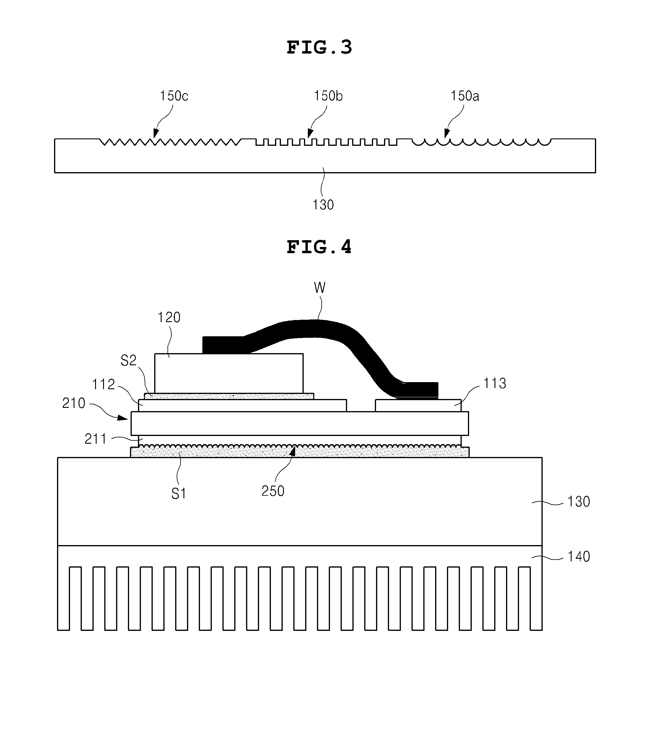
[0065]FIG. 4 is a view illustrating a power semiconductor module according to the present invention.

[0066]FIG. 4 shows a case in which a first uneven pattern 250 is formed on a surface of a first metal conductive track 211 of a substrate 210.

[0067]Also, in this case, the first uneven pattern 250 may be formed to have different shapes or different sizes or the same shape or size over the entire surface region or in a part of a region of the first metal conductive track 211.

[0068]When this structure is employed, a flux gas generated from a central portion of the substrate 210 can be easily discharged to the outside of the substrate 210 during a soldering process performed between the substrate 210 and the base plate 130, a generation of a non-junction portion or a void can be restrained, and a crack propagation speed in the solder S1 junction region can be drastically lowered due to the structural stabilization, in comparison to the related art, thus obtaining long-term reliability in...

third embodiment

[0069]FIG. 5 is a view illustrating a power semiconductor module according to the present invention.

[0070]FIG. 5 shows a case in which first uneven patterns 350a and 350b are formed on both surfaces of a first metal conductive track 311 of a substrate 310 and a base plate 330. In other words, the first uneven patterns 350a and 350b may be formed as a combination of the patterns of FIGS. 1 and 4.

[0071]In this case, the first uneven pattern 350a formed on the surface of first metal conductive track 311 may be finer than the first uneven patterns 350b formed on the surface of the base plate 330, but it may not necessarily do.

[0072]When this structure is employed, a flux gas generated from a central portion of the substrate 310 can be easily discharged to the outside of the substrate 310 during a soldering process performed between the substrate 310 and the base plate 330, a generation of a non-junction portion or a void can be restrained, and a crack propagation speed in the solder S1 ...


PUM


Abstract

Disclosed herein is a power semiconductor module including a substrate having a first metal conductive track formed on one surface thereof, and a base plate made of a metal and solder-joined to the substrate in the first metal conductive track region, wherein a first uneven pattern is formed in the solder junction region formed between the substrate and the base plate.

Description

CROSS REFERENCE TO RELATED APPLICATION[0001]This application claims the benefit of Korean Patent Application No. 10-2012-0131687, filed on Nov. 20, 2012, entitled “Power Semiconductor Module”, which is hereby incorporated by reference in its entirety into this application.BACKGROUND OF THE INVENTION[0002]1. Technical Field[0003]The present invention relates to a power semiconductor module.[0004]2. Description of the Related Art[0005]A power semiconductor module modularizes a power semiconductor such as an insulated gate bipolar mode transistor (IGBT), a metal oxide semi-conductor field effect transistor (MOSFET), or the like. Power semiconductor achieves high breakdown voltage characteristics, high current characteristics, and high frequency characteristics in comparison to a general semiconductor.[0006]The power semiconductor module is classified into a high power application and a low power application. For a high power application, a plurality of semiconductor elements is mounted...

Claims


Application Information

Patent Timeline
Patent Type & Authority Applications(United States)
IPC IPC(8): H01L23/48
CPCH01L23/36H01L23/3735H01L24/29H01L24/32H01L24/48H01L24/73H01L2224/29101H01L2224/32013H01L2224/32225H01L2224/48091H01L2224/48227H01L2224/48472H01L2224/73265H01L2224/83385H01L2924/00014H01L2924/13055H01L2924/13091H01L2924/15787H01L2924/00H01L2924/014H01L2224/45099H01L2924/00012
Inventor HA, JOBPARK, SANG HEE
Owner SAMSUNG ELECTRO MECHANICS CO LTD
Why Eureka
Try Eureka