Device for sealing and cooling multi-chip modules

a multi-chip module and sealing technology, applied in the direction of semiconductor devices, cooling/ventilation/heating modifications, semiconductor/solid-state device details, etc., to achieve the effects of high speed, reliable, and tight sealing

Inactive Publication Date: 2005-05-10
HITACHI LTD
View PDF22 Cites 26 Cited by
  • Summary
  • Abstract
  • Description
  • Claims
  • Application Information

AI Technical Summary

Benefits of technology

[0005]According to the present invention, techniques for sealing and cooling multi-chip modules equipped with a cooling mechanism are provided. Embodiments according to the invention can provide a reliable, tight seal for multi-chip modules with a high-density arrangement of multiple integrated circuit chips with semiconductor elements. Techniques according to the invention can eliminate, with a low thermal resistance, the heat generated by multiple integrated circuit chips with semiconductor elements. Embodiments according to the present invention can be especially useful when applied to integrated circuit chips with semiconductor elements, and more specifically for integrated circuit chips with semiconductor elements that provide high speeds, high integration, high heat-generation density, high power dissipation, and large dimensions for use in large-scale computers or supercomputers.

Problems solved by technology

Thus, providing a cooling mechanism to assure stable operations of the LSIs, and providing a tight sealing mechanism to reliably protect the LSIs from the outside environment are important technical issues for multi-chip modules.

Method used


Image

  • Device for sealing and cooling multi-chip modules
  • Device for sealing and cooling multi-chip modules
  • Device for sealing and cooling multi-chip modules

Examples


Embodiment Construction

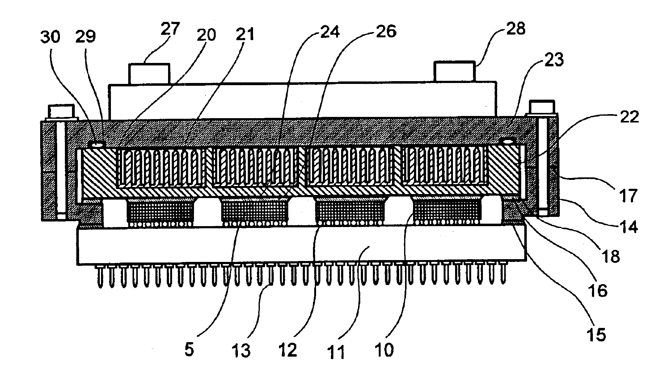
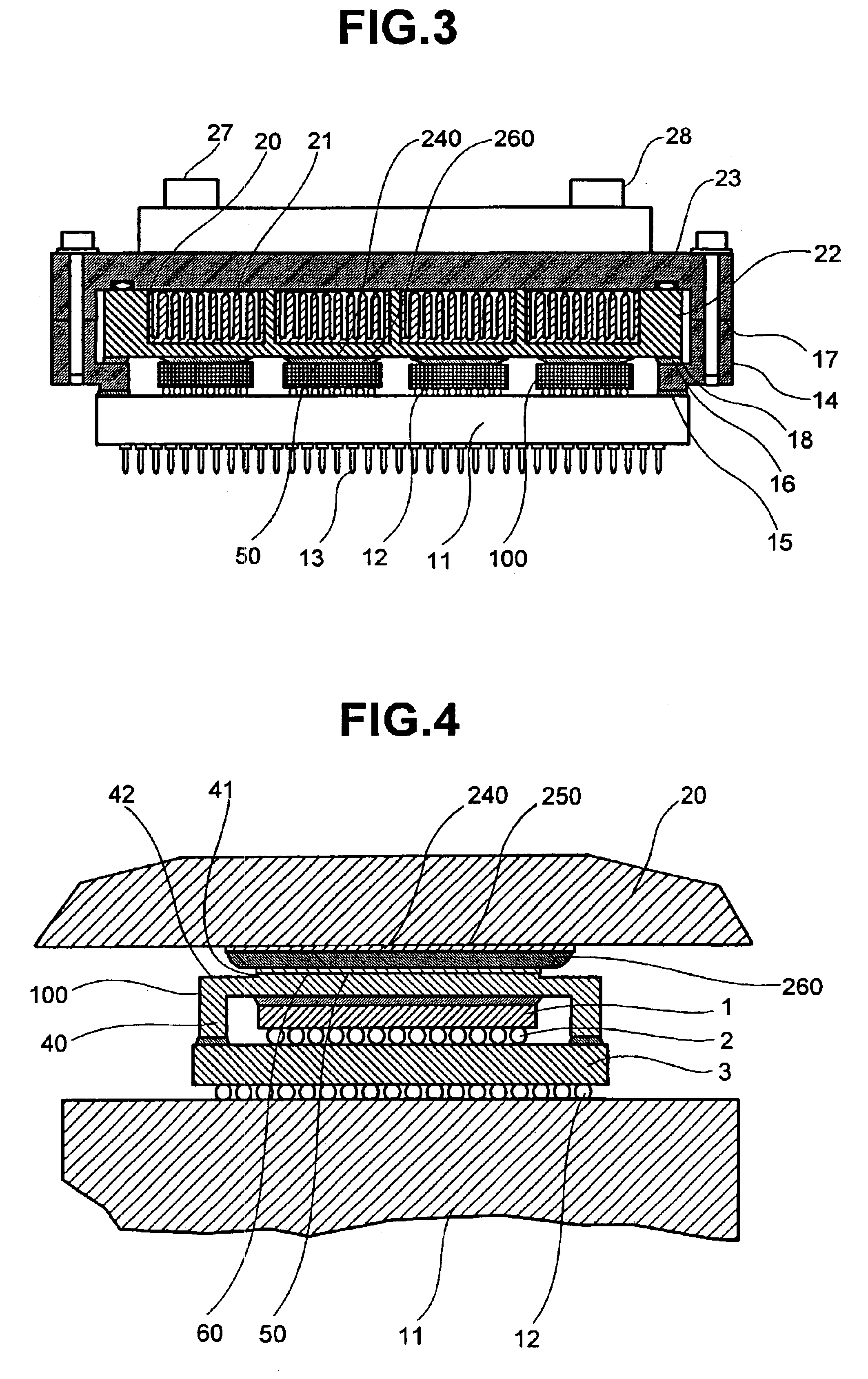
[0021]The present invention provides techniques for sealing and cooling multi-chip modules equipped with a cooling mechanism. Embodiments according to the invention can provide a reliable, tight seal for multi-chip modules with a high-density arrangement of multiple integrated circuit chips with semiconductor elements. Embodiments according to the present invention can be especially useful when applied to integrated circuit chips with semiconductor elements, and more specifically for integrated circuit chips with large-scale integrated circuits with semiconductor elements (hereinafter abbreviated as LSIs) that provide high speeds, high integration, high heat-generation density, high power consumption, and large dimensions for use in large-scale computers or supercomputers. In order to transfer signals at high-speeds between multiple LSIs, the electrical connections between the multiple LSIs must be made as short as possible. This need is met with multi-chip modules in which multiple...


PUM


Abstract

According to the invention, a sealing top plate in a multi-chip module is formed from a ceramic with high thermal conductivity having a thermal expansion coefficient consistent with that of a multi-layer circuit substrate. A cooling flow path cover covering the entirety of cooling flow path grooves is formed as a separate metallic member. The back surface of the sealing top plate, on which are formed the cooling flow path grooves, is bonded directly to the back surface of a semiconductor device using solder. A thermal-conductive jacket with low thermal resistance is provided. A multi-chip module sealing frame is soldered to the edge of the sealing top plate. Furthermore, a sealing material such as an O-ring is simply interposed between the edge of the sealing top plate and the cooling water path cover, and tightening means is used to tighten the metallic cooling flow path cover and the multi-chip module sealing frame to each other.

Description

CROSS-REFERENCES TO RELATED APPLICATIONS[0001]This application claims priority from Japanese Patent Application Reference No. 11-222058, filed Aug. 5, 1999, and is a continuation of application Ser. No. 09 / 631,889, filed Aug. 4, 2000, now U.S. Pat. No. 6,528,878.BACKGROUND OF THE INVENTION[0002]The present invention relates generally to integrated circuit chips with semiconductor elements, and more specifically for large scale integrated circuit chips with semiconductor elements that provide high speeds, high integration, high heat-generation density, high power dissipation, and large dimensions for use in large-scale computers or supercomputers.[0003]In computers, such as large-scale computers and supercomputers, increased processing throughput and storage capacity is achieved by higher speeds, greater integration, larger dimensions, and higher thermal density in large-scale integrated circuits with semiconductor elements (hereinafter abbreviated as LSIs). Also, in order to transfe...

Claims


Application Information

Patent Timeline
Patent Type & Authority Patents(United States)
IPC IPC(8): H01L23/02H01L23/10H01L23/473H01L23/34
CPCH01L23/10H01L23/473H01L2224/16H01L2224/73253H01L2924/09701H01L2924/15311H01L2924/15312H01L2924/01322H01L2924/16152H01L2924/16195H01L2924/1626
Inventor DAIKOKU, TAKAHIROKASAI, KENICHINETSU, TOSHITADAKOYANO, KOICHIUDA, TAKAYUKI
Owner HITACHI LTD
Why Eureka
Try Eureka