Thermal interface material layer and package-on-package device including the same

a technology of thermal interface material and package-on-package device, which is applied in the direction of semiconductor devices, semiconductor device details, electrical apparatus, etc., can solve the problems of reducing operation speed and suffering of pop devices, and achieve the effects of reducing failure of package-on-package devices, preventing cracks, and improving the yield of package-on-package devices

Active Publication Date: 2016-06-30
SAMSUNG ELECTRONICS CO LTD
View PDF6 Cites 15 Cited by
  • Summary
  • Abstract
  • Description
  • Claims
  • Application Information

AI Technical Summary

Benefits of technology

[0020]According to example embodiments of the inventive concept, a thermal interface material layer may be interposed between lower and upper semiconductor packages of a package-on-package device and be configured to have a specific physical property (for example, Mohs hardness lower than 7 and / or modulus of elasticity of 500 kPa or less). Accordingly, it is possible to prevent a crack from occurring in a lower semiconductor chip, when a solder ball joint process is performed to mount the upper semiconductor package on the lower semiconductor package. As a result, it is possible to reduce a failure of the package-on-package device and to improve a yield of the package-on-package device.
[0021]In addition, since the thermal interface material layer is added between the lower and upper semiconductor packages, it is possible to exhaust heat generated in the lower semiconductor chip quickly to the upper semiconductor package. As a result, it is possible to reduce a malfunction of the package-on-package device and to increase an operation speed of the package-on-package device.

Problems solved by technology

Since each package of the PoP device has a semiconductor chip and a package substrate, the PoP device has a large thickness causing various technical problems.
In addition, for the PoP device, it is difficult to exhaust heat generated in semiconductor chips to the outside, and thus, the PoP device suffers from technical problems, such as a device malfunction or a reduction in operation speed.

Method used


Image

  • Thermal interface material layer and package-on-package device including the same
  • Thermal interface material layer and package-on-package device including the same
  • Thermal interface material layer and package-on-package device including the same

Examples


embodiment 1

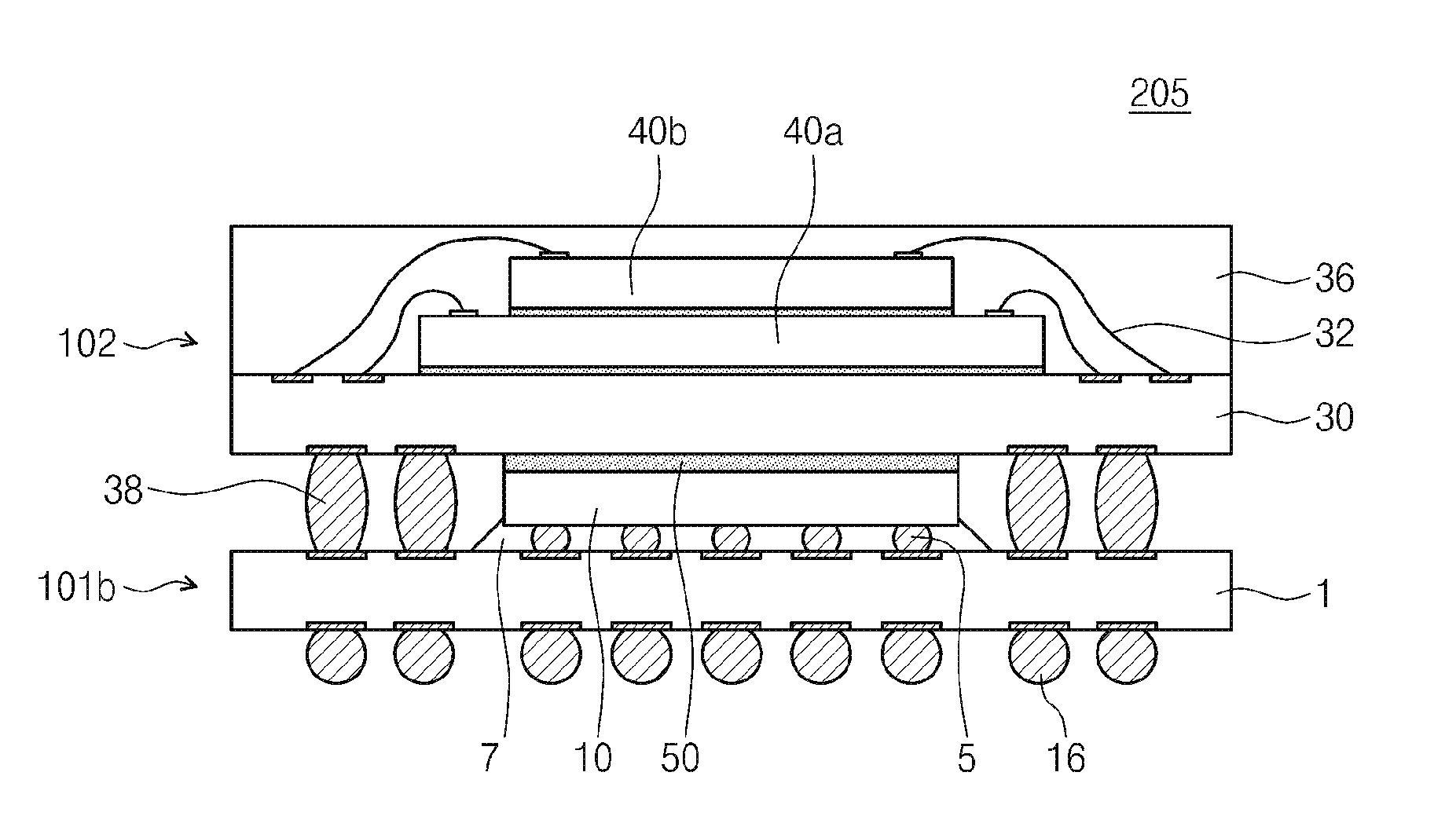
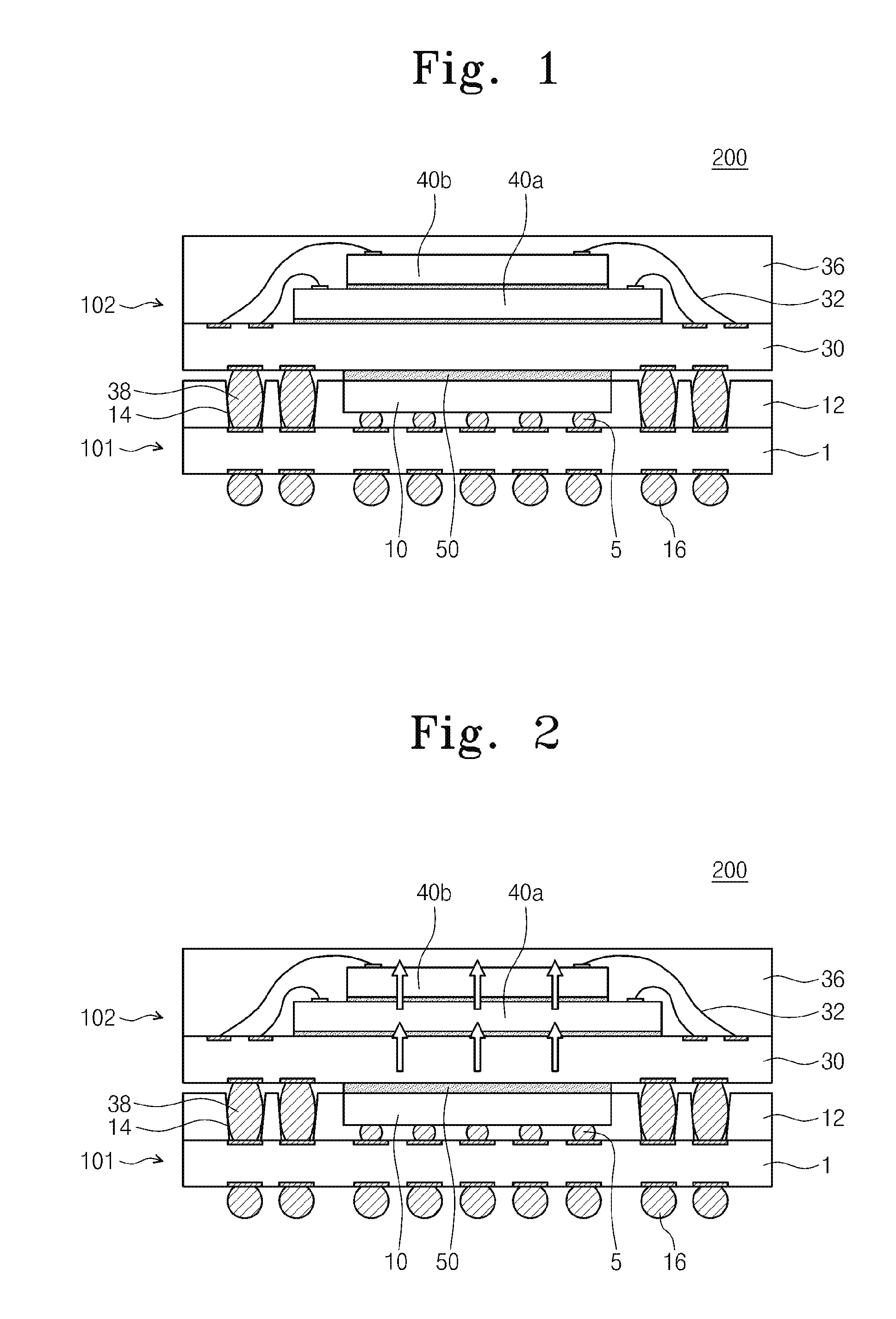
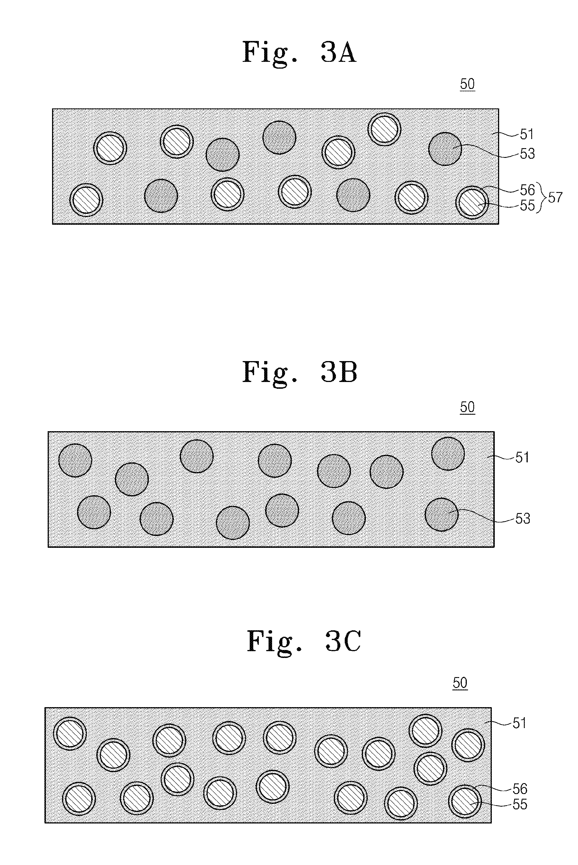
[0048]FIG. 1 is a sectional view illustrating an example of package-on-package devices according to example embodiment 1 of the inventive concept. FIG. 2 is a diagram illustrating a heat transfer process in a package-on-package device of FIG. 1. FIGS. 3A through 3C are sectional views exemplarily illustrating thermal interface material layers according to example embodiments of the inventive concept.

[0049]Referring to FIG. 1, a package-on-package device 200 according to the present embodiment 1 may include a lower semiconductor package 101 and an upper semiconductor package 102.

[0050]The lower semiconductor package 101 may include a lower package substrate 1, a lower semiconductor chip 10 mounted on the lower package substrate 1, and a lower mold layer 12 covering them. The lower semiconductor chip 10 may be electrically connected to the lower package substrate 1 in a flip-chip bonding manner using first lower solder bumps 5. Second lower solder bumps 16 may be provided under the lo...

first experimental example

[0076]In the first experimental example, a thermal interface material layer 165 was tested to know what relationship exists between insulation, crack, and scratch properties thereof and the type of filler particles contained therein. In the first experimental example, aluminum particle coated with aluminum oxide (Al2O3-coated Al), zinc oxide (ZnO), aluminum oxide (Al2O3), silicon oxide (SiO2), and silver (Ag) were used as the filler particle. A silicon-based material was used in common for the resin layer.

[0077](1) Insulation Property of a Thermal Interface Material Layer

[0078]FIG. 8 is a schematic diagram illustrating a circuit configuration for a first experimental example, in which insulation properties of thermal interface material layers according to example embodiments of the inventive concept are tested.

[0079]Referring to FIG. 8, conductive patterns 163 were formed on a substrate 161 to be spaced apart from each other. A space D1 between the conductive patterns 163 was 80 μm....

second experimental example

[0090]In the second experimental example, a relationship between a modulus of elasticity of the thermal interface material layer interposed between the lower and upper semiconductor packages and a yield of a package-on-package device was examined. In the second experimental example, the package-on-package devices 200 of FIG. 1 were formed by performing process steps described with reference to FIGS. 4 through 7. As shown in the following table 3, the package-on-package devices 200 were configured to include the thermal interface material layers having a modulus of elasticity ranging from 50 kPa to 120 MPa and then, yield thereof was examined. A change in modulus of elasticity of the thermal interface material layer was achieved by changing constituent, composition, and / or content of a resin layer of the thermal interface material layer. In the following table 3, a yield of 100% means there is no problem related to crack of the lower semiconductor chip, and a yield of 0% means that a...


PUM


Abstract

Provided are a thermal interface material layer and a package-on-package device including the same. The package-on-package device may include a thermal interface material layer interposed between lower and upper semiconductor packages and configured to have a specific physical property. Accordingly, it is possible to prevent a crack from occurring in a lower semiconductor chip, when a solder ball joint process is performed to mount the upper semiconductor package on the lower semiconductor package.

Description

TECHNICAL FIELD[0001]Example embodiments of the inventive concept relate to a thermal interface material layer and a package-on-package device including the same.BACKGROUND ART[0002]High-performance, high-speed and compact electronic systems are seeing increasing demand as the electronic industry matures. Various semiconductor package techniques have been proposed to meet such a demand. For example, a semiconductor package device may be configured to include a plurality of semiconductor chips mounted on a package substrate or to have a package-on-package (PoP) structure. Since each package of the PoP device has a semiconductor chip and a package substrate, the PoP device has a large thickness causing various technical problems. In addition, for the PoP device, it is difficult to exhaust heat generated in semiconductor chips to the outside, and thus, the PoP device suffers from technical problems, such as a device malfunction or a reduction in operation speed.DISCLOSURETechnical Prob...

Claims


Application Information

Patent Timeline
Patent Type & Authority Applications(United States)
IPC IPC(8): H01L23/373H01L25/065H01L23/367
CPCH01L23/373H01L25/065H01L23/367H01L23/49827H01L23/50H01L25/0657H01L21/563H01L24/16H01L24/32H01L24/48H01L24/73H01L24/92H01L25/105H01L25/50H01L2224/0401H01L2224/04042H01L2224/16225H01L2224/32145H01L2224/32225H01L2224/48091H01L2224/48227H01L2224/73204H01L2224/73253H01L2224/73265H01L2224/92225H01L2225/0651H01L2225/1023H01L2225/1058H01L2225/107H01L2225/1094H01L2924/15311H01L2924/15331H01L2924/18161H01L2225/06568H01L2924/181H01L2924/00014H01L2924/00012H01L2924/00H01L2224/45099H01L2224/45015H01L2924/207
Inventor NA, MIN-OKKIM, JONGKOOKRYU, HYO-CHANGPARK, JIN-WOOSON, BONGJINLEE, JANGWOO
Owner SAMSUNG ELECTRONICS CO LTD
Why Eureka
Try Eureka