Electrohydrodynamic (EHD) Printing for the Defect Repair of Contact Printed Circuits

a technology of electrohydrodynamic printing and contact printed circuits, which is applied in the direction of liquid/fluent solid measurement, fluid pressure measurement, peptides, etc., can solve the problem that the intended pattern transfer will never be completely accurate, and achieve the effect of removing discontinuity

Active Publication Date: 2014-06-12
SHARP KK
View PDF2 Cites 9 Cited by
  • Summary
  • Abstract
  • Description
  • Claims
  • Application Information

AI Technical Summary

Benefits of technology

[0014]It is reasonable to expect that the intended pattern transfer will never be completely accurate. A digital printing technology would be useful to repair defects that have occurred in a contact printed pattern. There are several established digital printing technologies in use for printed electronics including inkjet and electrohydrodynamic (EHD) printing. EHD has an advantage over conventional thermal and piezoelectric driven inkjet technologies because of the resolution that it is capable of printing. Typical printed feature sizes for conventional inkjet are around 30 μm, whereas EHD printed features are less than 10 μm. This makes EHD a suitable printing method for defect repair of contact printed features. The production of ink droplets in thermal and acoustically driven inkjet technologies is due to the interaction of a pressure wave in the ink with the nozzle opening at an edge of the ink chamber. This significantly limits the minimum size of the ink drops to be near the size of the nozzle opening. With EHD printing however, the ink drop is formed by the interaction of the charged ink with a powerful electrical field. It has been shown that the d...

Problems solved by technology

It is reasonable to expect that the intended ...

Method used


Image

  • Electrohydrodynamic (EHD) Printing for the Defect Repair of Contact Printed Circuits
  • Electrohydrodynamic (EHD) Printing for the Defect Repair of Contact Printed Circuits
  • Electrohydrodynamic (EHD) Printing for the Defect Repair of Contact Printed Circuits

Examples


Embodiment Construction

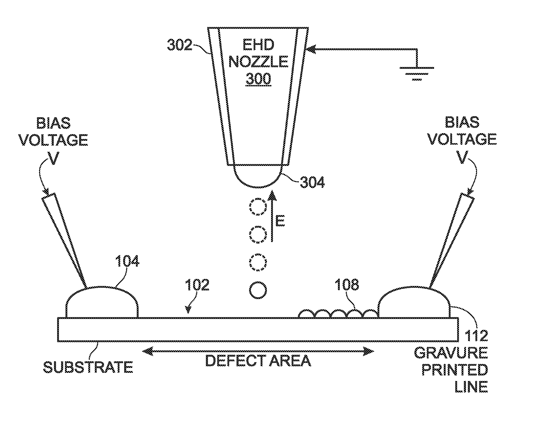
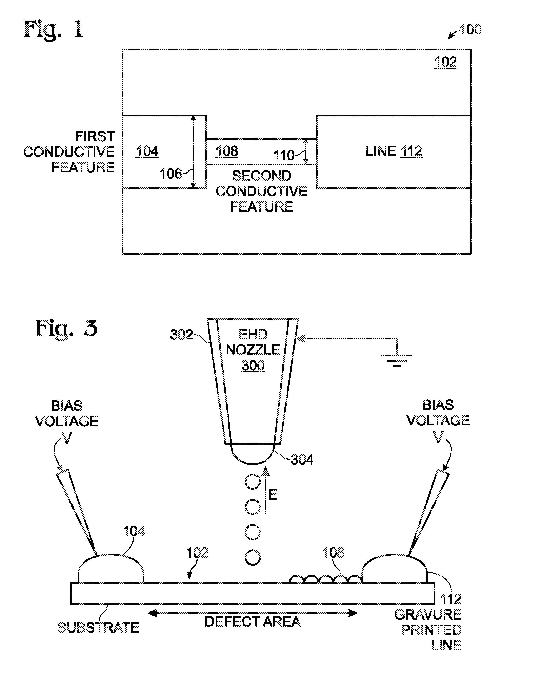
[0024]FIG. 1 is a plan view of a repaired contact printed circuit. The circuit 100 comprises a substrate with a top surface 102. A first conductive feature 104 overlies the substrate top surface 102 having a width 106 greater than about 5 microns. A second conductive feature 108 overlies the substrate top surface 102, and is electrically connected to the first conductive feature 104. The second conductive feature 108 has a width 110 of less than 1 micron. As shown, the first conductive feature 104 is a line, and the second conductive feature 108 is a line acting as a bridge to electrically connect the first conductive feature to another line 112. In other aspects not shown, a plurality of second features is formed in parallel between the first conductive feature 104 and line 112 to minimize resistance. Although straight lines have been depicted for simplicity, it should be understood that conductive features having a width of less than 1 micron can be formed between other conductive...


PUM

PropertyMeasurementUnit
Widthaaaaaaaaaa
Widthaaaaaaaaaa
Widthaaaaaaaaaa

Abstract

A method is provided for repairing defects in a contact printed circuit. The method provides a substrate with a contact printed circuit formed on a substrate top surface. After detecting a discontinuity in a printed circuit feature, a bias voltage is applying to at least one of a first region of the printed circuit feature or a second region of the printed circuit feature. The bias voltage may also be applied to both the first and second regions. An electric field is formed between the bias voltage and an ink delivery nozzle having a voltage potential less than the bias voltage. Conductive ink is attracted into the electric field from the ink delivery nozzle. Conductive is printed ink on the discontinuity, forming a conductive printed bridge. Typically, the ink delivery nozzle is an electrohydrodynamic (EHD) printing nozzle.

Description

BACKGROUND OF THE INVENTION[0001]1. Field of the Invention[0002]This invention generally relates to integrated circuit (IC) fabrication and, more particularly, to a method of repairing defects in contact printed electrical circuits using electrohydrodynamic (EHD) printing.[0003]2. Description of the Related Art[0004]As noted in Wikipedia, printed electronics is a set of printing methods used to create electrical devices on various substrates. Printing typically uses common printing equipment or other low-cost equipment suitable for defining patterns on material, such as screen printing, flexography, gravure, offset lithography and inkjet. Electrically functional electronic or optical inks are deposited on the substrate, creating for example, active or passive devices, such as thin film transistors or resistors. These processes can utilize any liquid phase material, including, but not limited to, solutions, mixtures, and dispersions containing organic semiconductors, inorganic semico...

Claims


Application Information

Patent Timeline
IPC IPC(8): H05K3/00H05K1/02
CPCH05K1/0213H05K3/00H05K3/225H05K3/125H05K2203/173
Inventor ULMER, KURTPUNTAMBEKAR, KANANSTECKER, LISA H.
Owner SHARP KK
Why Eureka
Try Eureka