Capacitive touch panel and fabrication method thereof
- Summary
- Abstract
- Description
- Claims
- Application Information
AI Technical Summary
Benefits of technology
Problems solved by technology
Method used
Image
Examples
Embodiment Construction
[0029]To provide a better understanding of the present disclosure, features of the embodiments will be made in detail. The embodiments of the present disclosure are illustrated in the accompanying drawings with numbered elements.
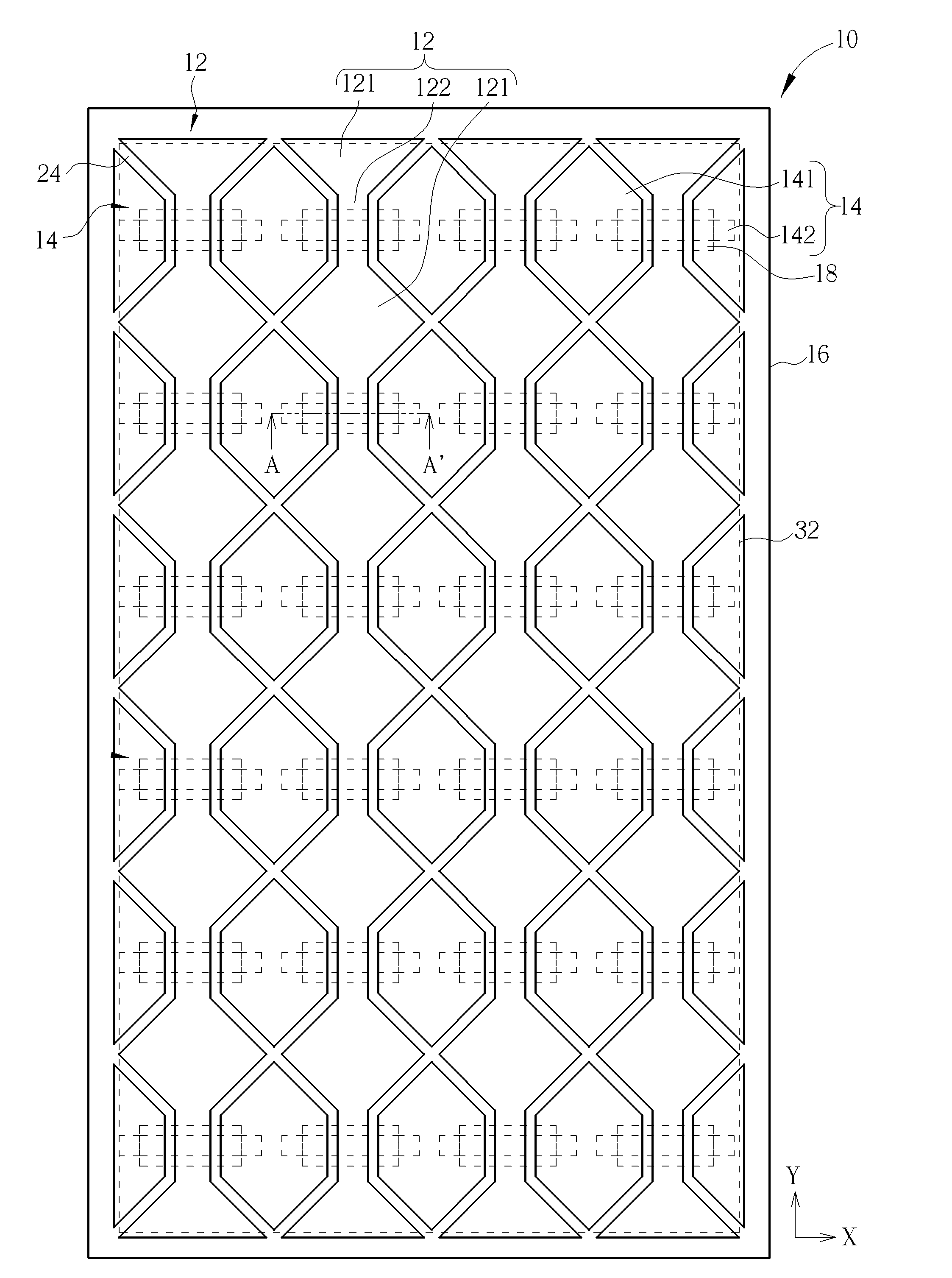
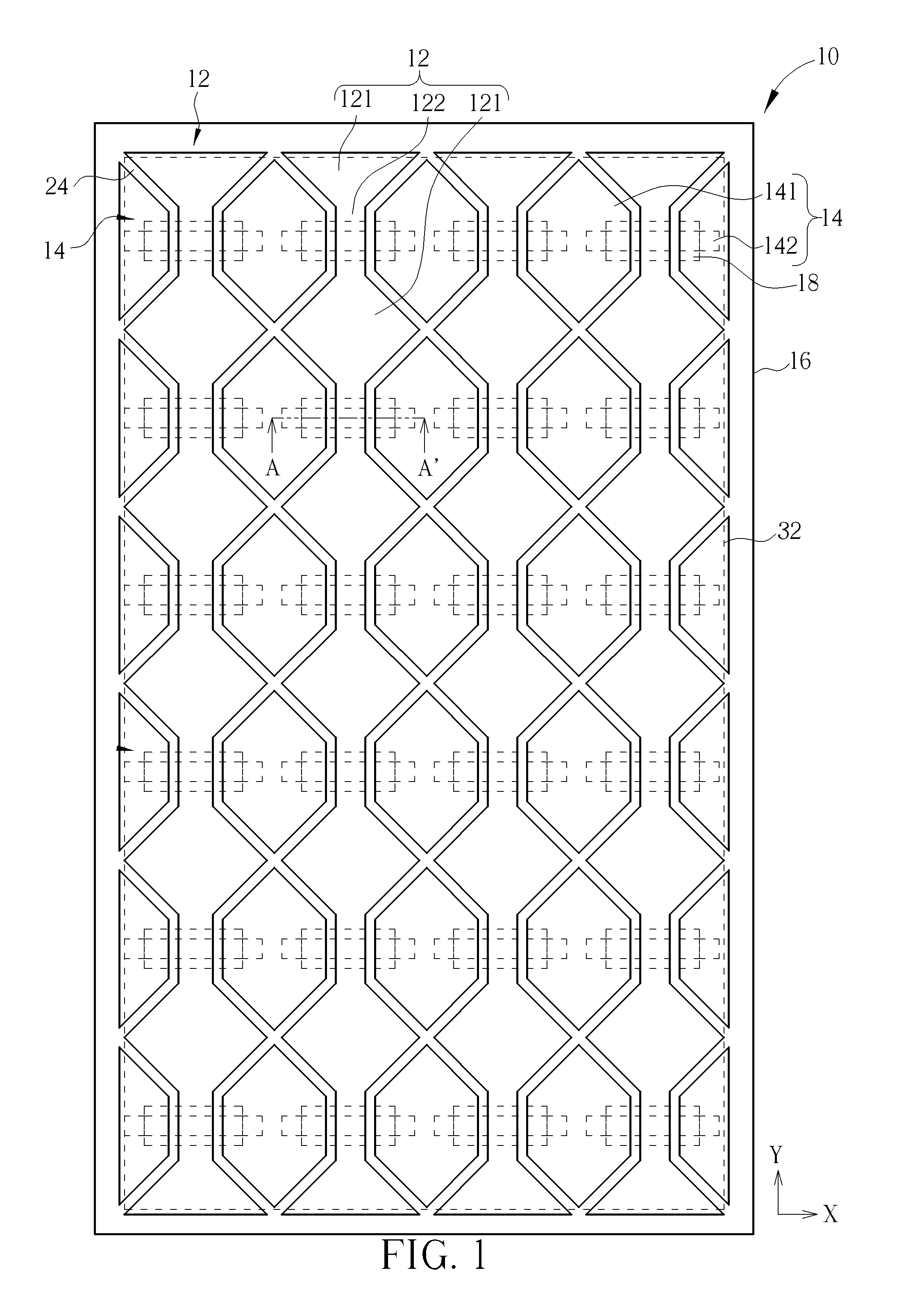
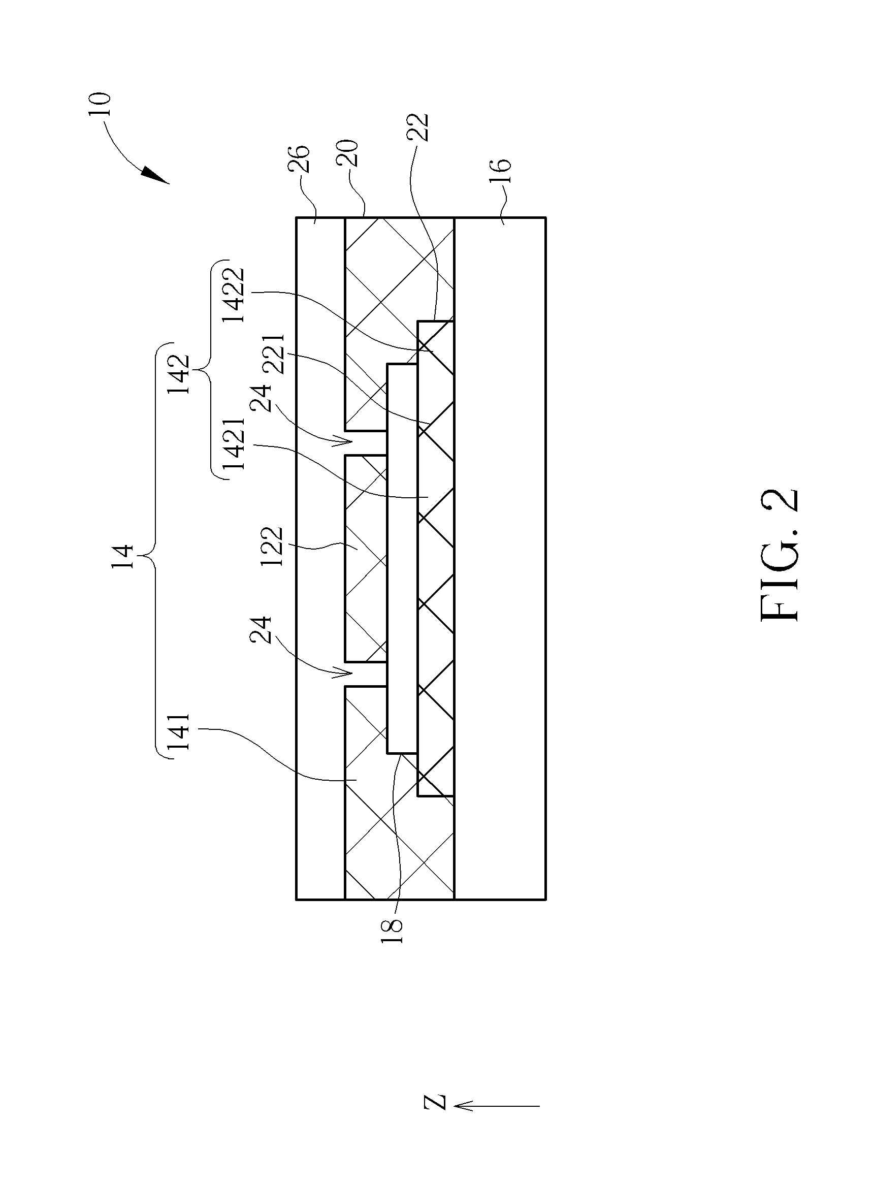
[0030]Referring to FIG. 1 and FIG. 2, FIG. 1 is a top-view schematic diagram locally illustrating a capacitive touch panel according to a first embodiment of the present invention, and FIG. 2 is a cross-sectional view diagram along a cross-sectional line A-A′ of the capacitive touch panel in FIG. 1. A capacitive touch panel 10 of the present invention includes a substrate 16, at least one first conductive series 14 and at least one second conductive series 12 disposed on the surface of the substrate 16. The substrate 16 may be a substrate composed of a soft material or a rigid material, such as a glass substrate, a strengthened glass substrate, a plastic substrate, a flexible cover lens, a flexible plastic substrate, for example, a plastic film, a thin glass...
PUM
 Abstract
Description
Claims
Application Information


