Electro-optical device and electronic apparatus

a technology of optical devices and electronic devices, applied in non-linear optics, instruments, optics, etc., can solve the problems of reducing display quality, affecting the quality of display, so as to achieve simple manufacturing process and long product life

Inactive Publication Date: 2014-06-12
SEIKO EPSON CORP
View PDF1 Cites 18 Cited by
  • Summary
  • Abstract
  • Description
  • Claims
  • Application Information

AI Technical Summary

Benefits of technology

[0021]In this case, it is possible to manufacture the electronic apparatus having the long product life with a relatively simple manufacturing process.

Problems solved by technology

In such a liquid crystal device, it is known that ionic impurities which are mixed into a liquid crystal material in a manufacturing process or ionic impurities which are generated by degradation of members due to light radiation or the like cause a decrease in display quality.
However, in a liquid crystal device disclosed in JP-A-11-38389 or JP-A-2000-338510, there is a problem that it is necessary for a high voltage to be continuously applied to the liquid crystal material for capturing the ionic impurities and temporal degradation is caused in the liquid crystal material.
That is, in the liquid crystal device disclosed in JP-A-11-38389 or JP-A-2000-338510, there is a problem that a decrease in the display quality cannot be avoided and product life of the liquid crystal device is limited.
On the other hand, in the configuration disclosed in JP-A-2007-249105, there is a problem that even though the decrease in the applied voltage can be suppressed, it is necessary to deposit a special material on the electrode and the manufacturing process is complicated.
As described above, in the liquid crystal device of the related art, there is a problem that it is difficult to achieve both a product life of the liquid crystal device and a simple manufacturing process thereof.

Method used


Image

  • Electro-optical device and electronic apparatus
  • Electro-optical device and electronic apparatus
  • Electro-optical device and electronic apparatus

Examples


embodiment 1

Overview of Electro-Optical Device

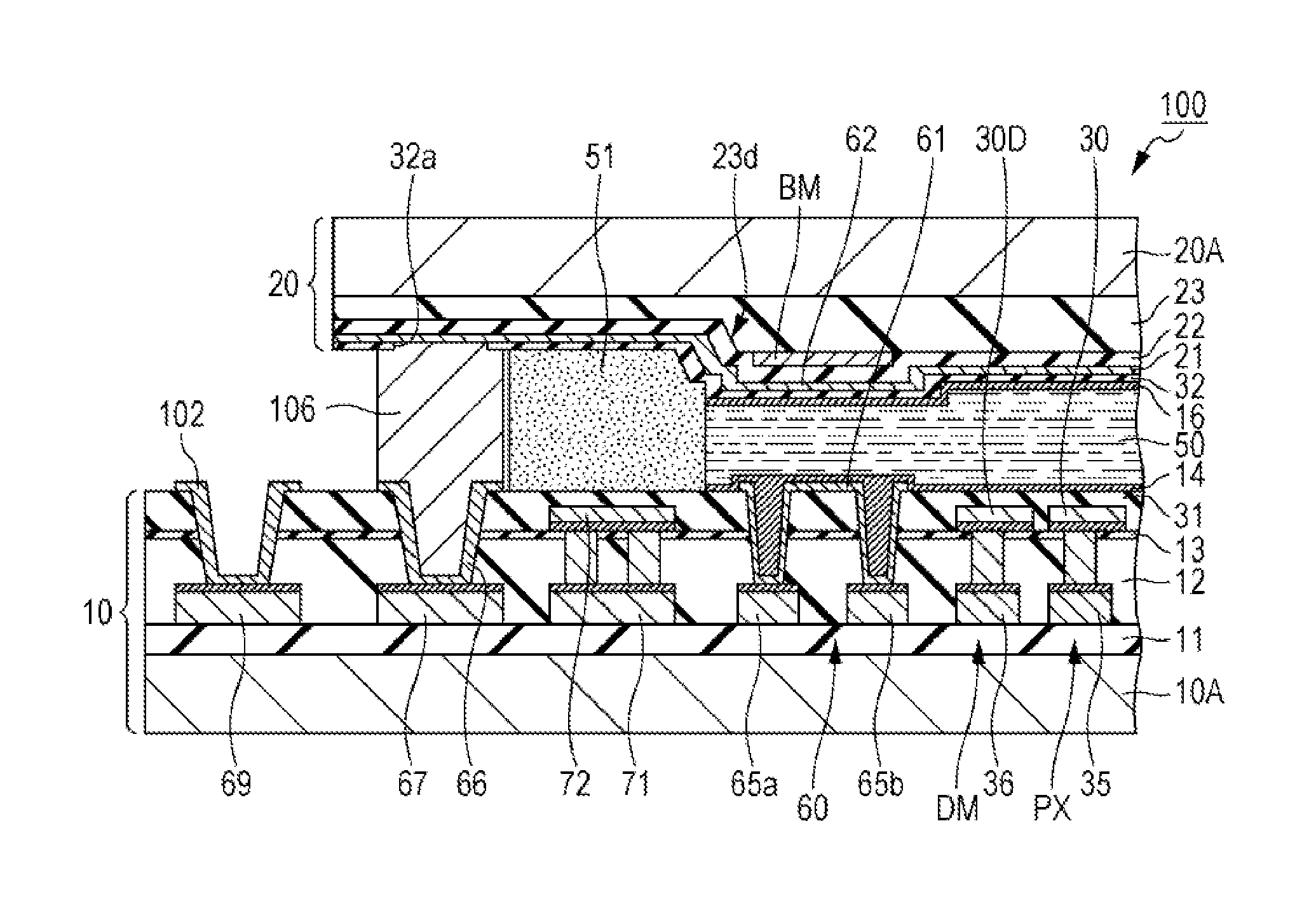
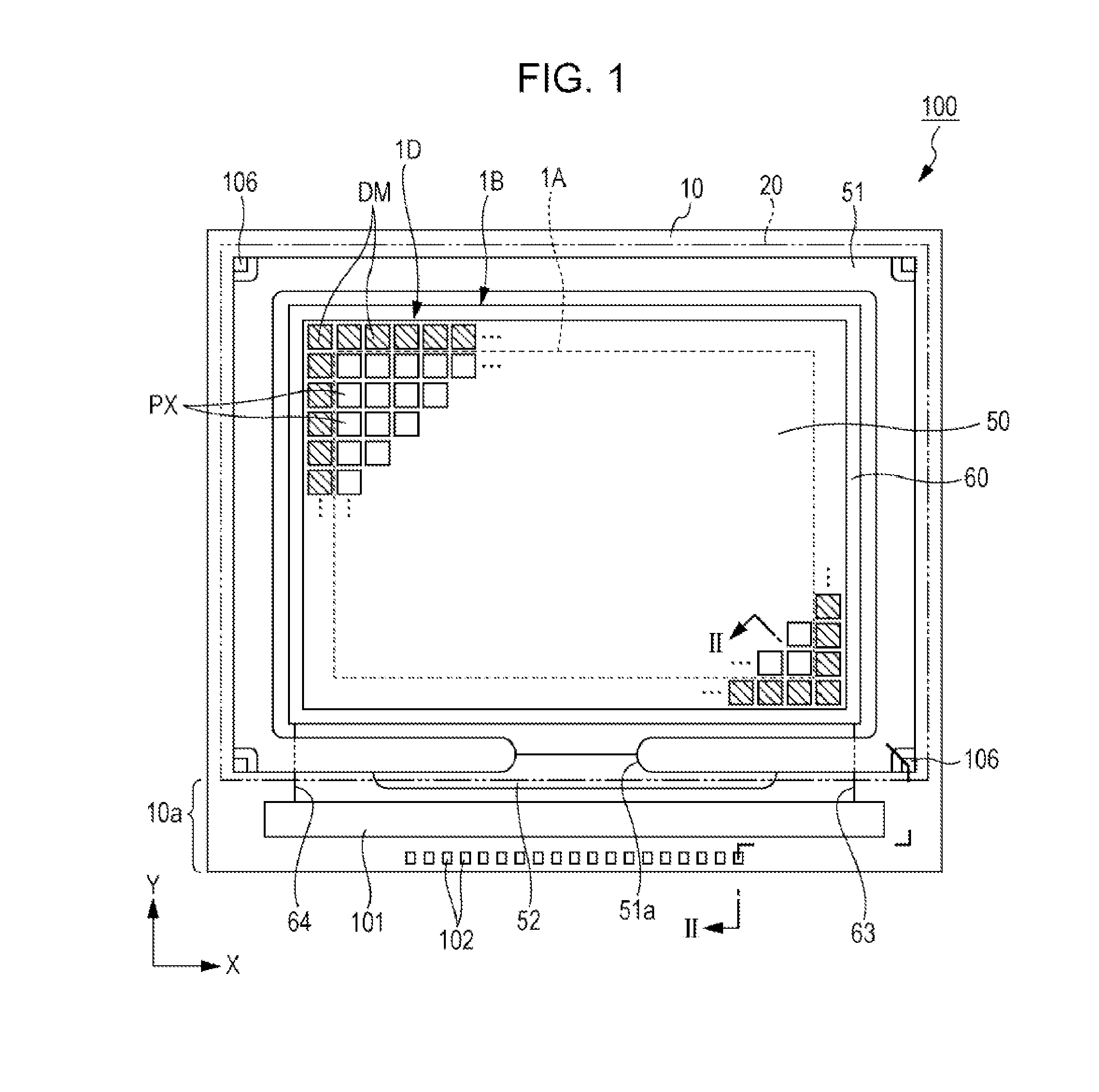
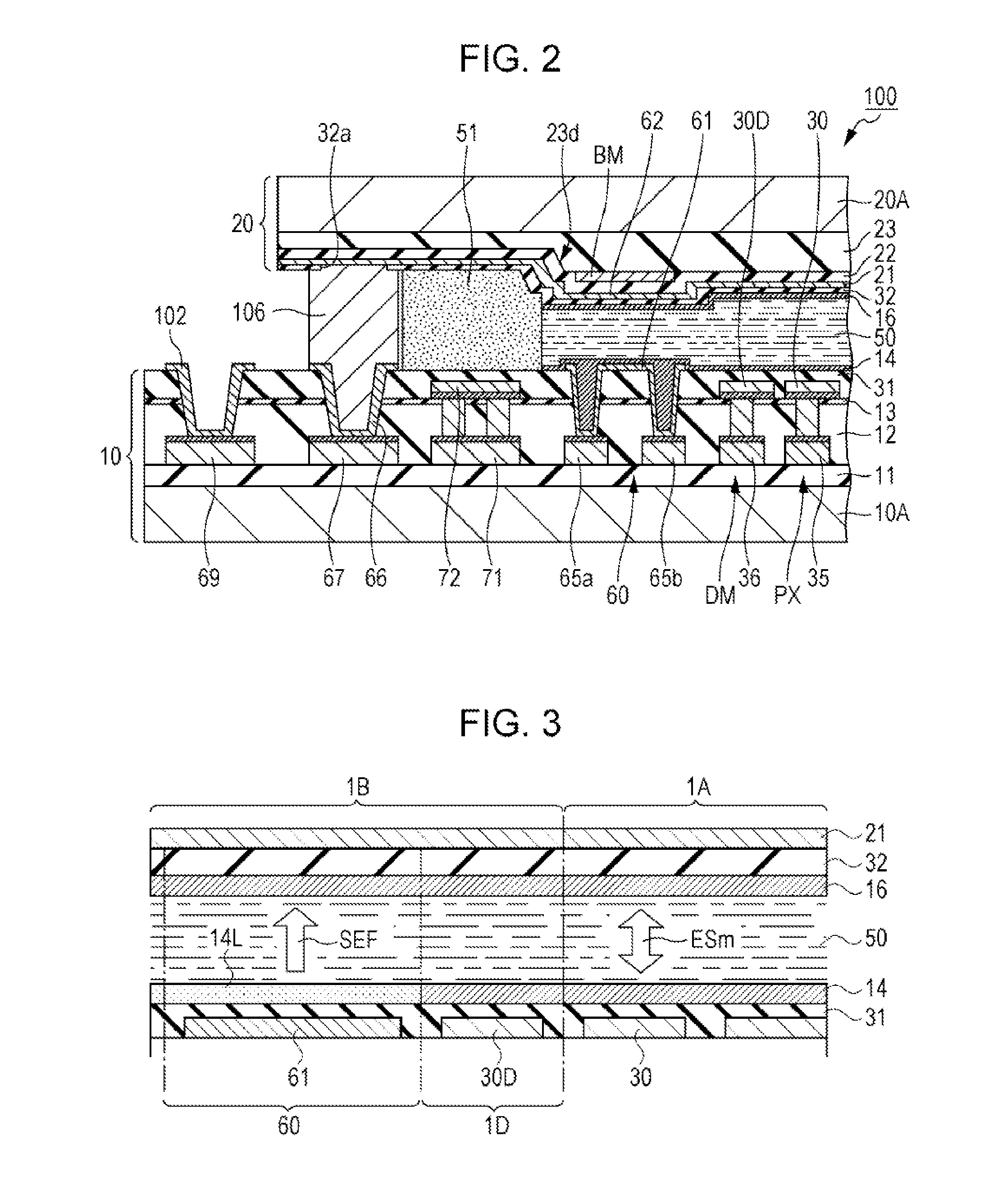
[0036]FIG. 1 is a plan view describing a configuration of a liquid crystal device. FIG. 2 is a partial cross-sectional view of the liquid crystal device in a position taken along line II-II illustrated in FIG. 1. First, a summary of an electro-optical device will be described with reference to FIGS. 1 and 2. In the embodiment, the electro-optical device is a reflective type liquid crystal device 100 and the liquid crystal device 100 includes a Thin Film Transistor (TFT) as the switching element of pixels. Furthermore, in the views which are referred to in the following description, an upper layer side or a surface side means a side (side on which an opposite substrate is positioned) opposite to a side on which a substrate body of an element substrate is positioned and a lower layer side means a side on which the substrate body of the element substrate is positioned, when describing a layer formed on the element substrate. In addition, an upper layer...

embodiment 2

Form Having Different Second Orientation Film

[0088]FIG. 6 is a schematic enlarged cross-sectional view of a liquid crystal device. Next, a form in which the second orientation film 16 is different from the embodiment 1 will be described with reference to FIGS. 6 and 4. In addition, for the same configuration parts as the embodiment 1, the same symbols are given and redundant description will be omitted.

[0089]In the embodiment (FIG. 6), forms of the first orientation film 14 and the second orientation film 16 are different from those of the embodiment 1 (FIG. 3). The other configurations are substantially the same as the embodiment 1. Even in such a configuration, the same effects as the embodiment 1 can be obtained. In the electro-optical device of the embodiment, as illustrated in FIG. 6, the density of the second orientation film 16 formed in the display region 1A is different from the density of the second orientation film 16 (in the embodiment, the second orientation film 16L ha...

embodiment 3

Form 1 Having Different First Orientation Film and Second Orientation Film

[0094]FIG. 7 is a schematic enlarged cross-sectional view of a liquid crystal device. Next, a form in which the first orientation film 14 and the second orientation film 16 are different from the embodiment 1 will be described with reference to FIG. 7. In addition, for the same configuration parts as the embodiments 1 and 2, the same symbols are given and redundant description will be omitted.

[0095]In the embodiment (FIG. 7), forms of the first orientation film 14 and the second orientation film 16 are different from those of the embodiment 1 (FIG. 3). The other configurations are substantially the same as the embodiment 1. Even in such a configuration, the same effects as the embodiment 1 can be obtained. In the electro-optical device of the embodiment, as illustrated in FIG. 7, the density of the first orientation film 14 formed in the display region 1A is different from the density of the first orientation ...


PUM

PropertyMeasurementUnit
thicknessaaaaaaaaaa
thicknessaaaaaaaaaa
frequencyaaaaaaaaaa

Abstract

An electro-optical device includes a first substrate, a second substrate and a liquid crystal, and has a display region and a peripheral region. The peripheral region of the first substrate has a peripheral electrode and a first orientation film covering the peripheral electrode. Then, since the density of first orientation film in the display region is different from the density of the first orientation film in the peripheral region, it is possible to efficiently capture ionic impurities present in the liquid crystal.

Description

BACKGROUND[0001]1. Technical Field[0002]The present invention relates to, for example, an electro-optical device and an electronic apparatus.[0003]2. Related Art[0004]A projector is an electronic apparatus which radiates light to a transmissive type electro-optical device or a reflective type electro-optical device and projects transmitted light or reflected light which is modulated by those electro-optical devices onto a screen. The projector is configured such that the light emitted from a light source is condensed and incident on the electro-optical device, and the transmitted light or the reflected light which is modulated depending on an electric signal is projected to be magnified onto the screen through a projection lens. The projector has an advantage of displaying a large screen. A liquid crystal device is known as the electro-optical device used in such an electronic apparatus and forms an image using dielectric anisotropy of the liquid crystal and optical rotation of ligh...

Claims


Application Information

Patent Timeline
Patent Type & Authority Applications(United States)
IPC IPC(8): G02F1/1337
CPCG02F1/1337G02F1/134309G02F2201/501G02F1/133388
Inventor NISHIDA, MASAKAZU
Owner SEIKO EPSON CORP
Why Eureka
Try Eureka