

Touch sensor integrated type display device
a display device and touch sensor technology, applied in the field can solve the problems of user dissatisfaction, reduced visibility of display devices, increased thickness of display devices, etc., and achieve the effects of reducing the change amount of capacitance generated by the common electrode, reducing the thickness of touch sensor integrated type display devices, and reducing the thickness of display devices
- Summary
- Abstract
- Description
- Claims
- Application Information
AI Technical Summary
Benefits of technology
Problems solved by technology
Method used
Image

Examples
first embodiment
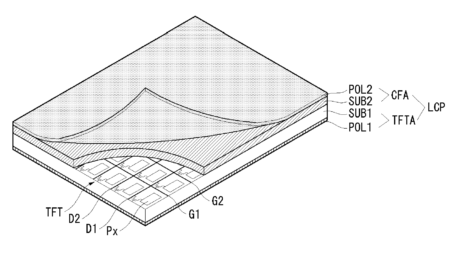
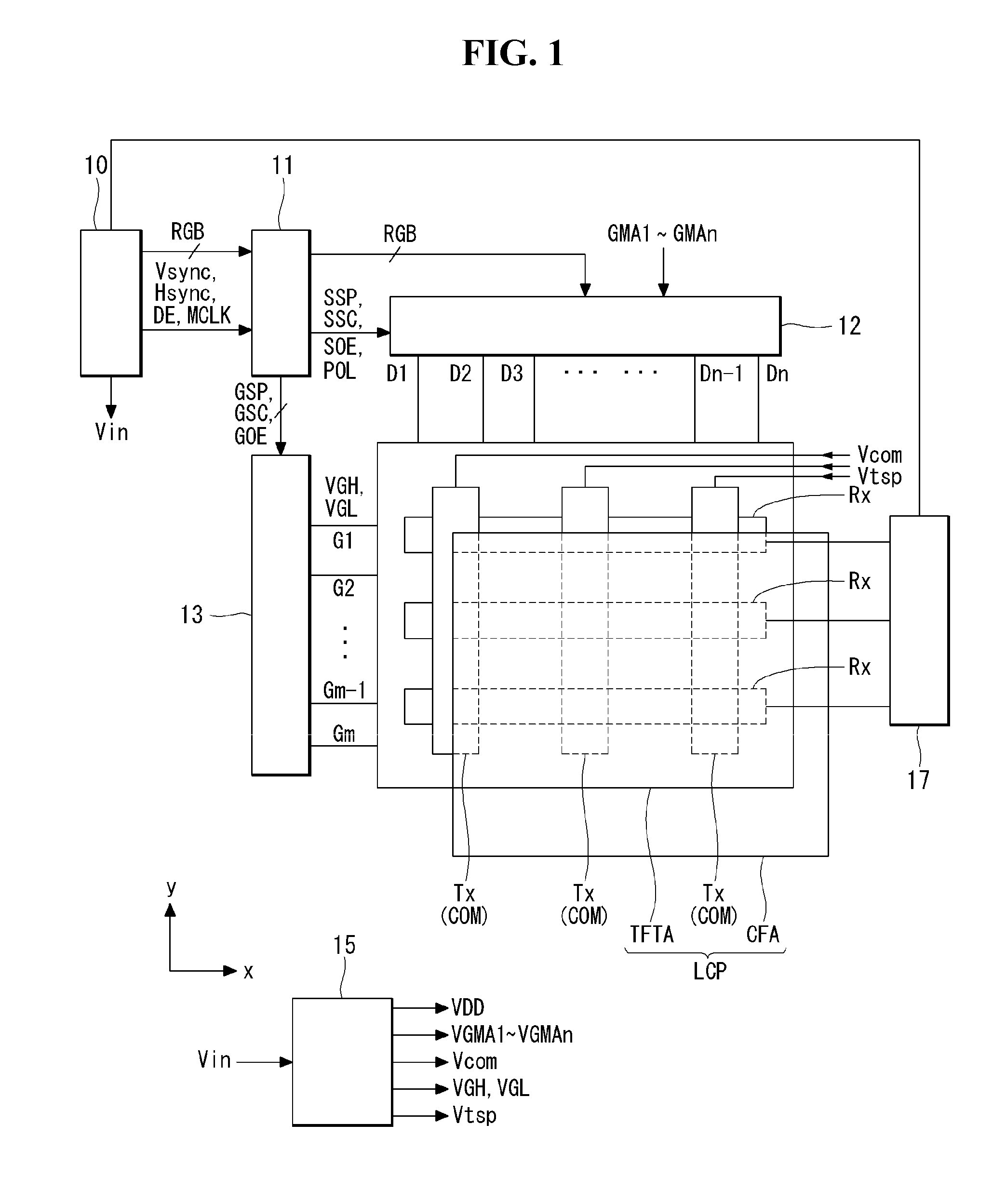
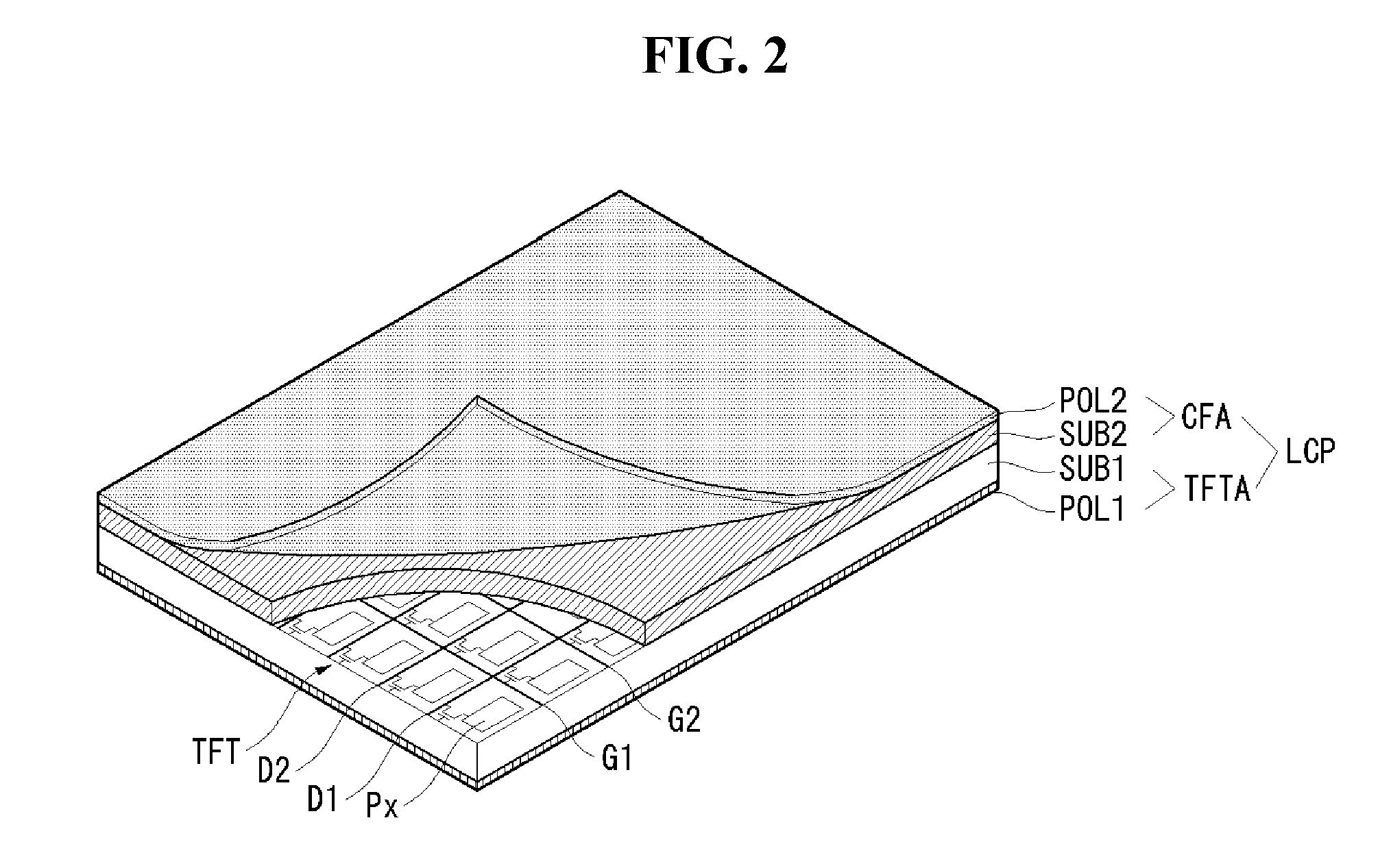
[0034]As shown in FIG. 1, a touch sensor integrated type liquid crystal display according to the invention includes a liquid crystal display panel LCP, a host controller 10, a timing controller 11, a data driver 12, a gate driver 13, a power supply unit 15, and a touch recognition processor 17.
[0035]The liquid crystal display panel LCP includes a color filter array CFA and a thin film transistor (TFT) array TFTA which are positioned opposite each other with a liquid crystal layer (not shown) interposed therebetween.
[0036]As shown in FIGS. 1 and 2, the TFT array TFTA includes a plurality of gate lines G1, G2, . . . , Gm which are formed in parallel on a first substrate SUB 1 in a first direction (for example, x-axis direction), a plurality of data lines D1, D2, . . . , Dn which are formed in parallel in a second direction (for example, y-axis direction) to cross the plurality of gate lines G1, G2, . . . , Gm, thin film transistors TFT formed at crossings of the gate lines G1, G2, . ....
second embodiment
[0052]As shown in FIGS. 5 and 6A, a thin film transistor (TFT) array TFTA according to the invention includes gate lines GL and data lines DL which are formed on a first substrate SUB1 to cross over each other, thin film transistors TFT formed at crossings of the gate lines GL and the data lines DL, pixel electrodes Px formed in areas defined by a crossing structure of the gate lines GL and the data lines DL, touch driving electrodes Tx formed between the pixel electrodes Px, which are adjacent to each other with the gate line GL interposed therebetween, common electrodes COM serving as a touch sensing electrode positioned opposite the pixel electrodes Px, and first and second shielding electrodes Sx1 and Sx2 which are formed between the common electrode COM serving as the touch sensing electrode and the touch driving electrode Tx to form an electric field along with the common electrode COM. Hence, the first and second shielding electrodes Sx1 and Sx2 reduce an influence of the ele...
PUM
 Abstract
Description
Claims
Application Information