Soft pin insertion during physical design

Inactive Publication Date: 2014-07-03
GLOBALFOUNDRIES US INC
View PDF1 Cites 6 Cited by
  • Summary
  • Abstract
  • Description
  • Claims
  • Application Information

AI Technical Summary

Benefits of technology

[0009]The present invention is generally directed to a method of stabilizing or controlling placement of logic such as an architectural logic path in an integrated circuit design by receiving a circuit description of the design which include an input net of the logic path and an output net of the logic path, designating the logic path as a region for which placement stability is desired, inserting in the circuit description at least first and second virtual (soft) pins wherein the first virtual pin has a first fixed location proximate the input net and is interconnected with the input net and the second virtual pin has a second fixed location proxi

Problems solved by technology

An IC may include a very large number of cells and require complicated connections between the cells.
Due to the large number of components and the details required by the fabrication process for very large scale integrated (VLSI) devices, physical design is not practical without the aid of computers.
However, physical synthesis can take days to complete

Method used


Image

  • Soft pin insertion during physical design
  • Soft pin insertion during physical design
  • Soft pin insertion during physical design

Examples


Embodiment Construction

)

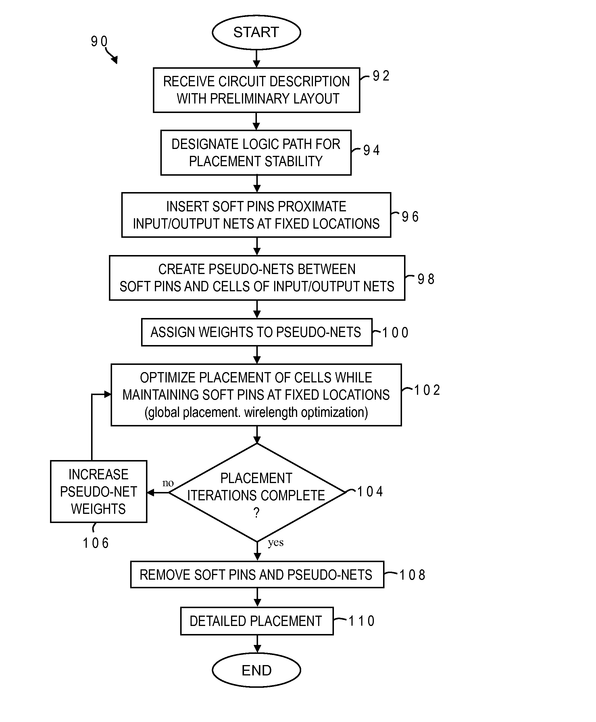
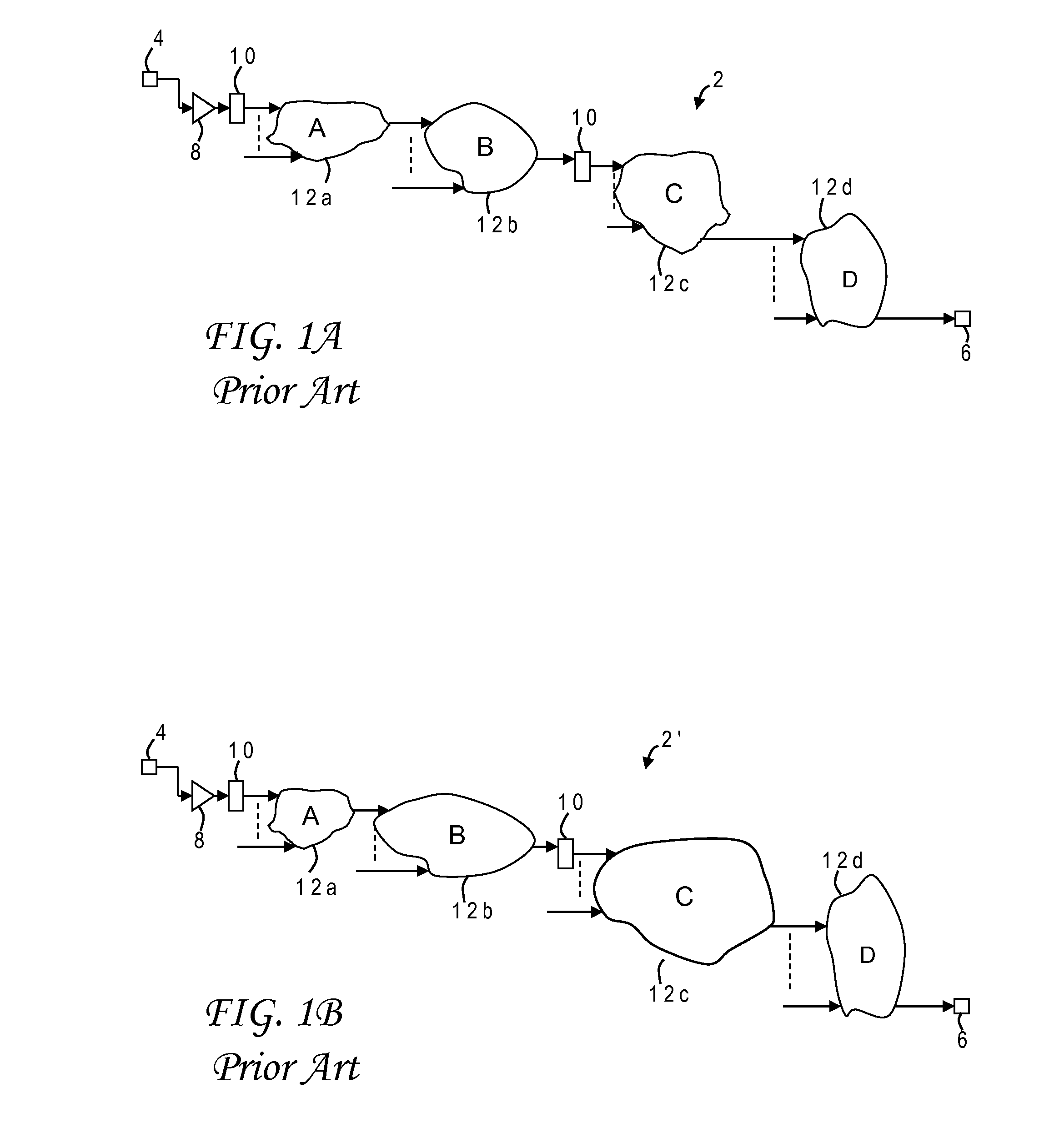
[0020]Current microprocessor trends are integrating traditionally custom designs with random logic macros (RLMs) into very large integrated circuit designs. In some cases, entire microprocessor units are designed using an automated synthesis flow that integrates these traditional custom designs and RLMs. This type of merged synthesis run is referred to as large block synthesis (LBS). The LBS blocks, i.e., sets of cells or logic modules, require handling dataflow designs differently than traditional RLMs. In particular, as the size of the designs grow, it takes significant effort to make synthesis generate architecturally correct placement solutions due to placement instability as problems with timing and congestion are incrementally solved. Slight changes to the assertions in the circuit design can drastically modify the placement solution, creating new timing problems that where not there before. Balanced timing is often not achieved until the product development phase becomes sta...


PUM


Abstract

A netlist for an integrated circuit design is constrained by virtual or “soft” pins to control or stabilize the placement of logic such as an architectural logic path. One soft pin is inserted at a fixed location proximate an input net of the path and is interconnected with the input net, and another is inserted at a fixed location proximate the output net and is interconnected with the output net. Cell placement is then optimized while maintaining the virtual pins at their fixed locations. More than two virtual pins may be inserted to bound a cluster of logic. The virtual pins may lie along the input/output nets. Pseudo-net weights are assigned to pseudo-nets formed between a cell and the virtual pins, and the pseudo-net weight can be increased for each placement iteration.

Description

BACKGROUND OF THE INVENTION[0001]1. Field of the Invention[0002]The present invention generally relates to the design of semiconductor chips and integrated circuits, and more particularly to a method of placing components of an integrated circuit design in a layout.[0003]2. Description of the Related Art[0004]Integrated circuits are used for a wide variety of electronic applications, from simple devices such as wristwatches, to the most complex computer systems. A microelectronic integrated circuit (IC) chip can generally be thought of as a collection of logic cells with electrical interconnections between the cells, formed on a semiconductor substrate (e.g., silicon). An IC may include a very large number of cells and require complicated connections between the cells. A cell is a group of one or more circuit elements such as transistors, capacitors, resistors, inductors, and other basic circuit elements combined to perform a logic function. Cell types include, for example, core cel...

Claims


Application Information

Patent Timeline
IPC IPC(8): G06F17/50
CPCG06F17/5077G06F30/392
Inventor VISWANATH, MANIKANDANWARD, SAMUEL I.
Owner GLOBALFOUNDRIES US INC
Why Eureka
Try Eureka