Organic light emitting diode display and manufacturing method thereof

a technology of light-emitting diodes and organic light-emitting diodes, which is applied in the direction of thermoelectric device junction materials, electrical equipment, and semiconductor devices, etc., can solve the problems of reducing the thickness deteriorating the transfer quality, and reducing the height of the pixel definition layer, so as to increase the transfer quality of the organic emission layer

Active Publication Date: 2014-07-10
SAMSUNG DISPLAY CO LTD
View PDF2 Cites 5 Cited by
  • Summary
  • Abstract
  • Description
  • Claims
  • Application Information

AI Technical Summary

Benefits of technology

[0010]Embodiments of the present invention provide an organic light emitting diode (OLED) display directed toward increasing transfer quality of an organic emission layer by minimizing protrusions and depressions at a bottom of the organic emission layer due to transfer direction when the organic emission layer is formed according to a laser induced thermal imaging method, and a manufacturing method thereof.

Problems solved by technology

There is a limit to reducing the thickness of the pixel definition layer formed with an organic layer due to material or process characteristics, and the pixel definition layer may not have uniformity of height.
Also, when the donor film is disposed on the substrate on which the pixel definition layer is formed and an organic emission layer with a specific color is transferred by continuously irradiating laser beams in a second direction, the organic emission layer generates a large curve near a part of the pixel definition layer (which is placed depending on the first direction), thereby deteriorating transfer quality.

Method used


Image

  • Organic light emitting diode display and manufacturing method thereof
  • Organic light emitting diode display and manufacturing method thereof
  • Organic light emitting diode display and manufacturing method thereof

Examples


Embodiment Construction

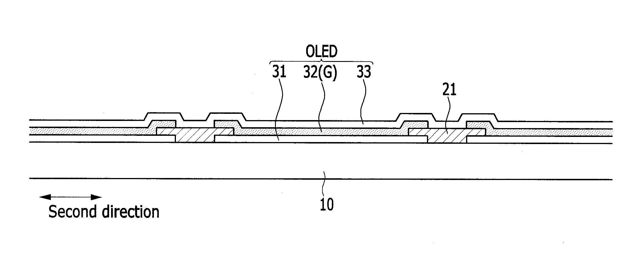
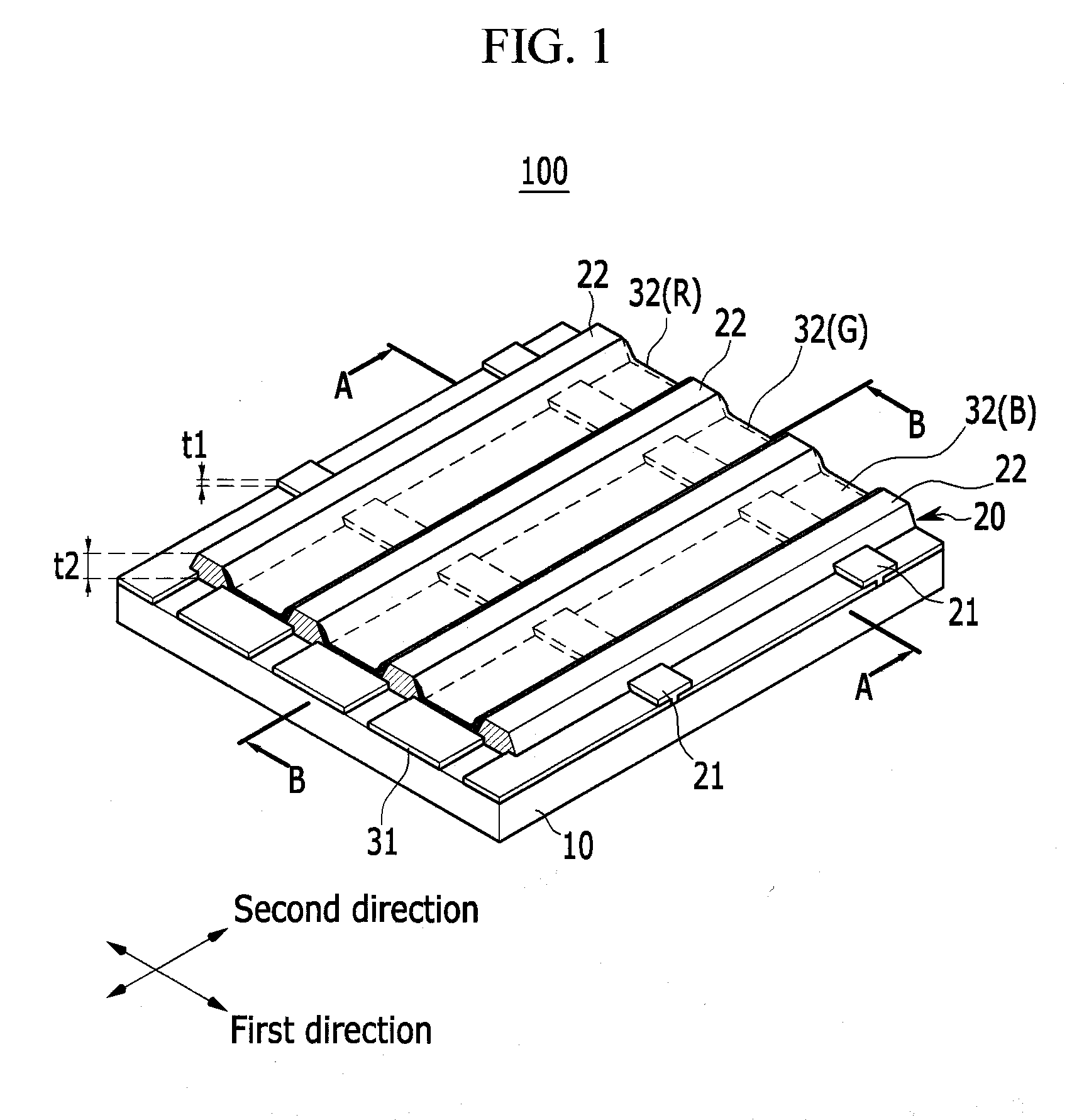
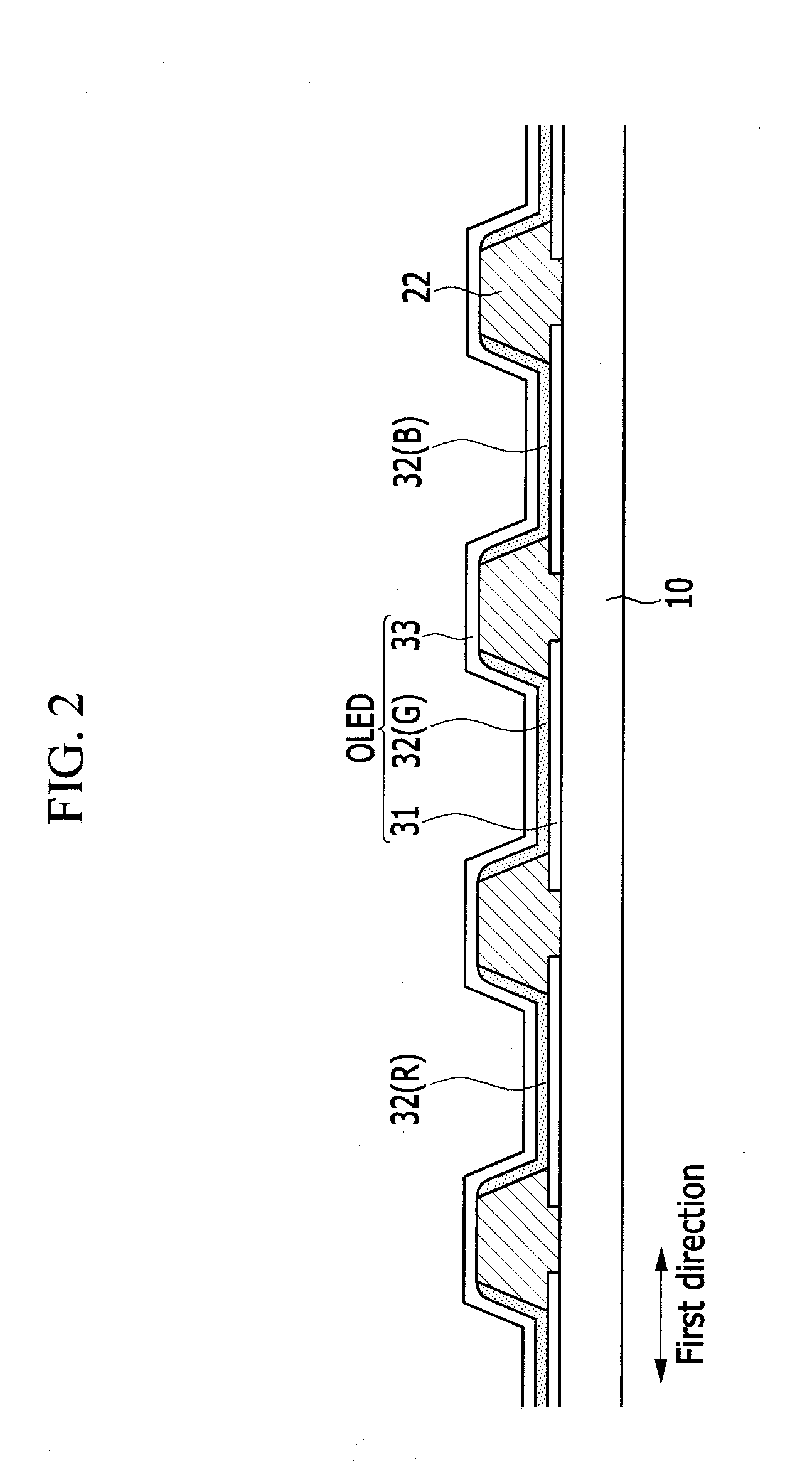
[0035]The present invention will be described more fully hereinafter with reference to the accompanying drawings, in which exemplary embodiments of the invention are shown. As those skilled in the art would realize, the described embodiments may be modified in various different ways, all without departing from the spirit or scope of the present invention.

[0036]Herein, unless explicitly described to the contrary, the word “comprise” or “include” and variations such as “comprises”, “includes”, “comprising”, or “including” will be understood to imply the inclusion of stated elements but not the exclusion of any other elements. When it is said that any element, such as a layer, film, region, or electrode, is positioned on another element, the element may be directly on the other element or one or more intermediate elements may be interposed therebetween. In addition, an upper part of a target portion indicates an upper part or a lower part of the target portion, and it does not mean tha...


PUM


Abstract

An organic light emitting diode (OLED) display includes: pixel electrodes formed on a substrate; a pixel definition layer between the pixel electrodes and partitioning a pixel area; organic emission layers of a plurality of colors on the pixel electrodes; and a common electrode on the organic emission layers. The pixel definition layer includes a first pattern and a second pattern having different formation materials, thicknesses, and extension directions.

Description

CROSS-REFERENCE TO RELATED PATENT APPLICATIONS[0001]This application claims priority to and the benefit of Korean Patent Application No. 10-2013-0002544, filed in the Korean Intellectual Property Office on Jan. 9, 2013, the entire content of which is incorporated herein by reference.BACKGROUND[0002]1. Field[0003]Embodiments of the present invention relate to an organic light emitting diode (OLED) display including a pixel definition layer, and a manufacturing method thereof.[0004]2. Description of the Related Art[0005]An organic light emitting diode display includes a plurality of pixels, and an organic light emitting diode (OLED) is included in each pixel. Each pixel is surrounded by a pixel definition layer and is distinguished (or separated) from neighboring pixels. The OLED includes a pixel electrode for each pixel, an organic emission layer on the pixel electrode, and a common electrode on a substrate.[0006]The organic emission layer may include a red organic emission layer, a ...

Claims


Application Information

Patent Timeline
Patent Type & Authority Applications(United States)
IPC IPC(8): H01L27/32H01L51/56H01L51/52
CPCH01L27/3206H01L51/56H01L51/5284H01L51/5203H10K59/30H10K59/173H10K59/122H10K2102/351
Inventor KIM, JUN-YOUNG
Owner SAMSUNG DISPLAY CO LTD
Why Eureka
Try Eureka