Semiconductor light-emitting device

a technology semiconductor light-emitting device, which is applied in the direction of semiconductor devices, basic electric elements, electrical appliances, etc., can solve the problems of reducing and undesired empty spaces between semiconductor light-emitting device and other problems, to achieve the effect of increasing heat resistance and reliability of semiconductor light-emitting devi

Active Publication Date: 2014-07-31
SAMSUNG ELECTRONICS CO LTD
View PDF1 Cites 53 Cited by
  • Summary
  • Abstract
  • Description
  • Claims
  • Application Information

AI Technical Summary

Benefits of technology

[0004]Exemplary embodiments of the inventive concept provides a semiconductor light-emitting device which may increase heat resistance and the reliability of the semiconductor light-emitting device by minimizing empty spaces remaining between a package substrate and the semiconductor light-emitting device on which stepped portions are formed.

Problems solved by technology

After the semiconductor light-emitting device is bonded to the package substrate by using the eutectic die bonding, undesired empty spaces may remain between the semiconductor light-emitting device and the package substrate due to stepped portions on the semiconductor light-emitting device.
The undesired empty spaces may reduce heat resistance and the reliability of the semiconductor light-emitting device.

Method used


Image

  • Semiconductor light-emitting device
  • Semiconductor light-emitting device
  • Semiconductor light-emitting device

Examples


Embodiment Construction

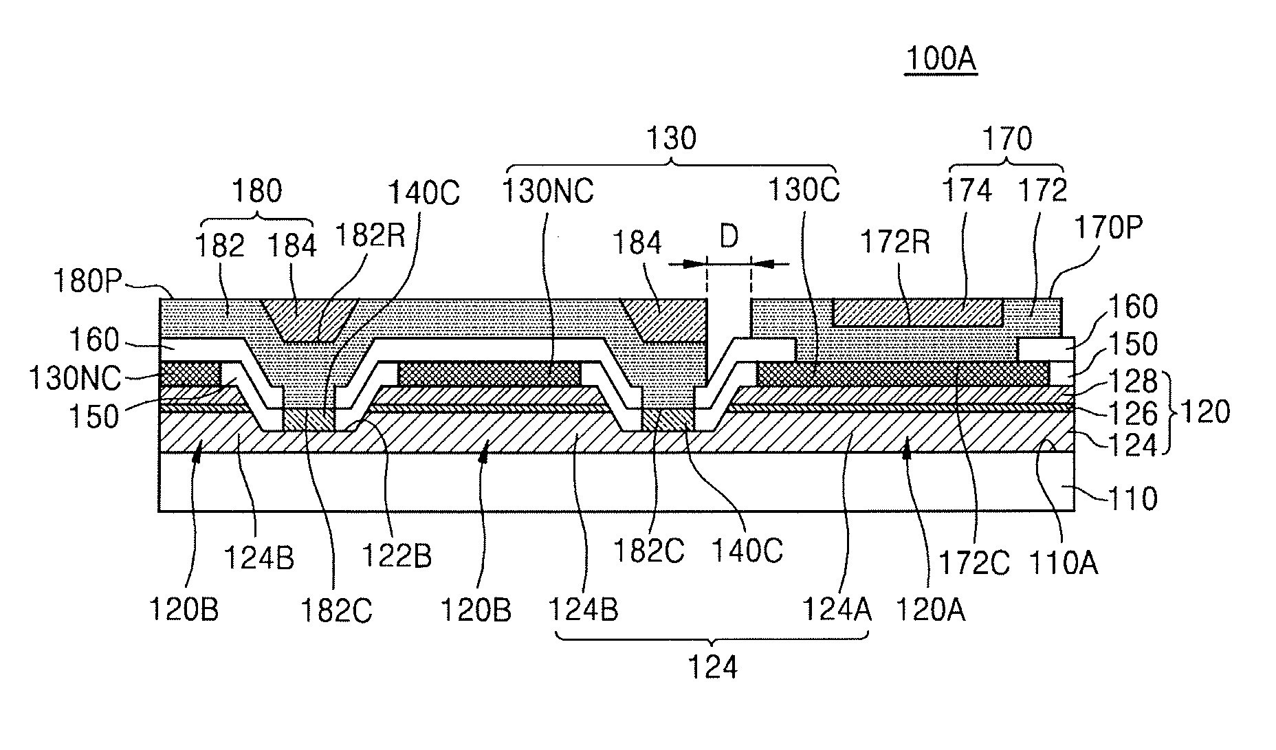
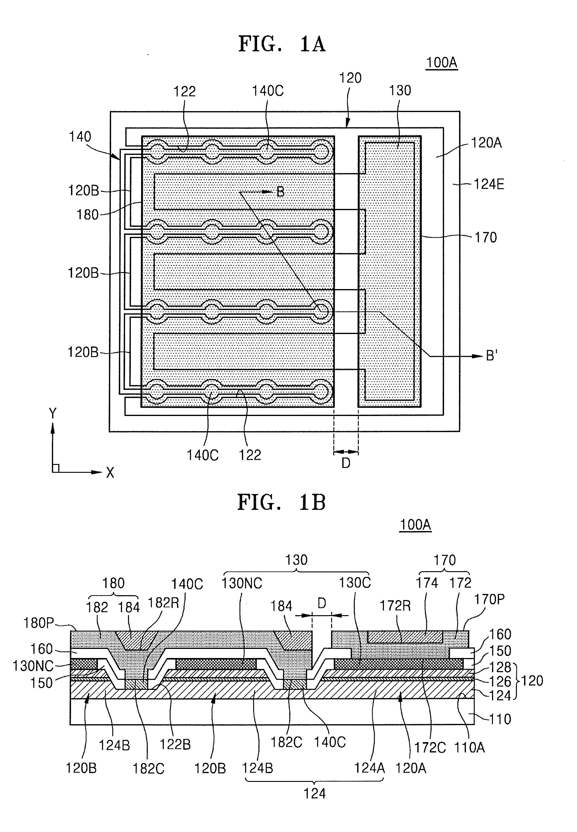
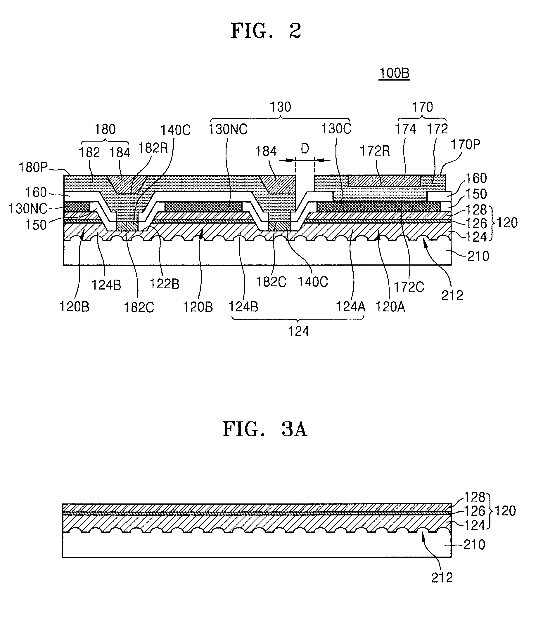
[0038]Exemplary embodiments of the inventive concept will now be described more fully with reference to the accompanying drawings, in which exemplary embodiments of the invention are shown. Exemplary embodiments of the invention may, however, be embodied in many different forms and should not be construed as being limited to embodiments set forth herein.

[0039]The terminology used herein is for the purpose of describing particular embodiments only and is not intended to be limiting of exemplary embodiments of the invention. As used herein, the singular forms “a”, “an” and “the” are intended to include the plural forms as well, unless the context clearly indicates otherwise.

[0040]In addition, as used herein, the term “and / or” includes any and all combinations of one or more of the associated listed items.

[0041]In the drawings, the same elements are denoted by the same reference numerals and a repeated explanation thereof will not be given. Also, in the drawings, the size and relative ...


PUM


Abstract

A semiconductor light-emitting device includes a light-emitting structure that includes a first conductive semiconductor layer, an active layer, a second conductive semiconductor layer, an electrode layer contacting one of the first conductive semiconductor layer and the second conductive semiconductor layer, and a bonding conductive layer connected to the electrode layer. The bonding conductive layer includes a main bonding layer having a recess area defined by a stepped portion on a surface opposite to a surface facing the electrode layer, and a filling bonding layer filling at least a part of the recess area.

Description

CROSS-REFERENCE TO RELATED APPLICATIONS[0001]This application claims priority to Korean Patent Application No. 10-2013-0010101, filed on Jan. 29, 2013 the disclosure of which is hereby incorporated by reference herein in its entirety.(I) TECHNICAL FIELD[0002]The present disclosure relates to a semiconductor light-emitting device, and more particularly, to a semiconductor light-emitting device that is mounted on a package substrate by using flip-chip technology.(II) DISCUSSION OF THE RELATED ART[0003]Light-emitting diodes (LEDs) using a nitride semiconductor (nitride semiconductor light-emitting devices) are widely used in various light sources such as, for example, lighting devices, signal lamps, and large display devices used for backlighting. As the light-emitting diode (LED) market for illumination has expanded and products having high reliability, high efficiency, and high output may be required, a flip-chip bonding technology using eutectic die bonding, which is a high heat dis...

Claims


Application Information

Patent Timeline
Patent Type & Authority Applications(United States)
IPC IPC(8): H01L33/38
CPCH01L33/38H01L33/20H01L33/22H01L33/44H01L33/62H01L2924/0002H01L2933/0016H01L2924/00H01L33/36
Inventor KIM, TAE-HUNLEE, SEUNG-HWAN
Owner SAMSUNG ELECTRONICS CO LTD
Why Eureka
Try Eureka