Monitor, touchscreen sensing module thereof, and method for manufacturing the touchscreen sensing module

a touchscreen sensing module and monitor technology, applied in the field of electromechanical technology, can solve the problems of increasing cost, environmental pollution, waste of ito, etc., and achieve the effects of avoiding environmental pollution, reducing costs, and avoiding material was

Active Publication Date: 2014-08-07
ANHUI JINGZHUO OPTICAL DISPLAY TECH CO LTD
View PDF6 Cites 10 Cited by
  • Summary
  • Abstract
  • Description
  • Claims
  • Application Information

AI Technical Summary

Benefits of technology

[0036]Firstly, the first conductive layer and the second conductive layer of the touchscreen sensing module are respectively received in the first groove and the second groove, and the first conductive layer and the second conductive layer respectively match with the first groove and the second groove in shape. Therefore, no etching process is needed to obtain electrodes when forming conductive layers, which avoids from wasting of material and reduces costs.
[0037]Secondly, because no etching process is needed during manufacturing the touchscreen sensing module. Therefore, it avoids from using of chemical substances, and thereby avoids environmental pollution.

Problems solved by technology

ITO is a kind of expensive material, and patterning results in a large amount of waste of ITO, thereby increasing the cost.
Besides, corrosive chemical materials are used in etching process, which causes environmental pollution.

Method used


Image

  • Monitor, touchscreen sensing module thereof, and method for manufacturing the touchscreen sensing module
  • Monitor, touchscreen sensing module thereof, and method for manufacturing the touchscreen sensing module
  • Monitor, touchscreen sensing module thereof, and method for manufacturing the touchscreen sensing module

Examples


Embodiment Construction

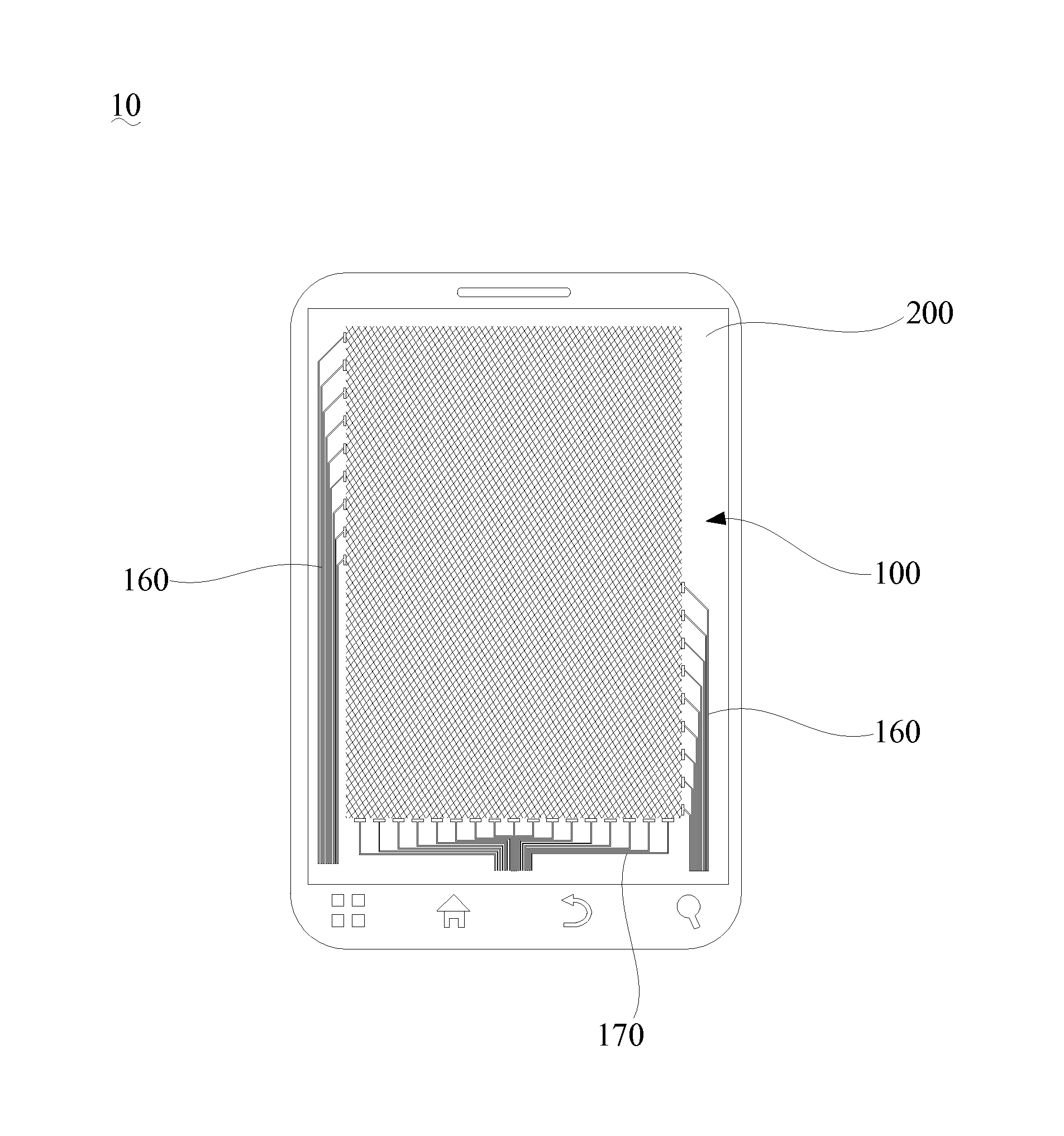
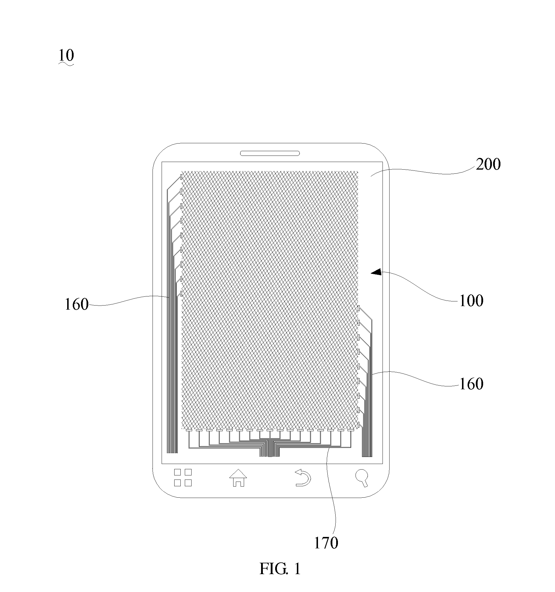
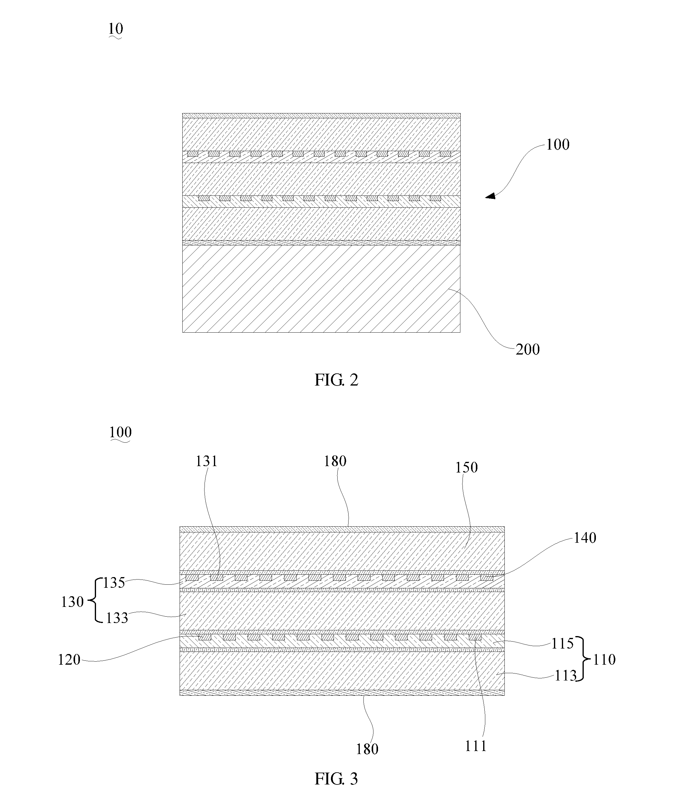
[0047]The disclosure is described more fully hereinafter with reference to the accompanying drawings, in which preferred embodiments of the invention are shown. The disclosure may, however, be embodied in many different forms and should not be construed as limited to the embodiments set forth herein. Rather, these embodiments are provided so that this disclosure will be thorough and complete.

[0048]It should be noted that, when an element is described as “fixed to” another element, it means the element can be fixed to another element directly or with a middle element. When an element is described as “connected to” another element, it means the element can be connected to another element directly or with a middle element.

[0049]Unless defined elsewhere, all the technology and science terms used herein should be with the same meaning as understood by those skilled in the art. All the terms used herein are just for the purpose of describing detailed embodiments, but not limited to the sc...


PUM

PropertyMeasurementUnit
widthaaaaaaaaaa
thicknessaaaaaaaaaa
widthaaaaaaaaaa

Abstract

A touchscreen sensing module includes a first baseplate, a first conductive layer, a second baseplate, a second conductive layer, and a supporting substrate. A first groove in a predetermined shape is defined on a side of the first baseplate. The first conductive layer matches with the first groove in shape, and the first conductive layer is received in the first groove. A second groove in a predetermined shape is defined on a side of the second baseplate. The second conductive layer matches with the second groove in shape, and the second conductive layer is received in the second groove. The first conductive layer and the second conductive layer respectively match with the first groove and the second groove in shape, no etching is needed to obtain electrodes when forming the conductive layers, which avoids material waste and reduces costs In addition, a monitor is also provided by the present invention.

Description

FIELD OF THE INVENTION[0001]The present disclosure relates to electronic technology, and more particularly relates to a monitor, a touchscreen sensing module, and a method for manufacturing the touchscreen sensing module.BACKGROUND OF THE INVENTION[0002]Touchscreen is a sensing device capable of receiving touch input signals. The touchscreen brings a new appearance for information exchange and is a new attractive information interactive device. For conventional touchscreens, ITO (Indium Tin Oxide) conductive layer is still a much important part.[0003]When manufacturing ITO conductive layer, an ITO film is coated on an entire surface of a substrate, ITO patterning is then carried out to obtain electrodes, and transparent electrode silver leads are finally made. In ITO patterning, the formed ITO film is etched by etching process. ITO is a kind of expensive material, and patterning results in a large amount of waste of ITO, thereby increasing the cost. Besides, corrosive chemical mater...

Claims


Application Information

Patent Timeline
Patent Type & Authority Applications(United States)
IPC IPC(8): G02F1/1333
CPCG02F1/13338G06F3/04164G06F3/0445G06F3/0446G06F2203/04112H05K3/107H05K3/1258H05K3/4611H05K2201/09681H05K2201/10128Y10T29/49105
Inventor GAO, YULONG
Owner ANHUI JINGZHUO OPTICAL DISPLAY TECH CO LTD
Why Eureka
Try Eureka