

Methods and structures for reducing stress on die assembly
- Summary
- Abstract
- Description
- Claims
- Application Information
AI Technical Summary
Benefits of technology
Problems solved by technology
Method used
Image

Examples
Embodiment Construction
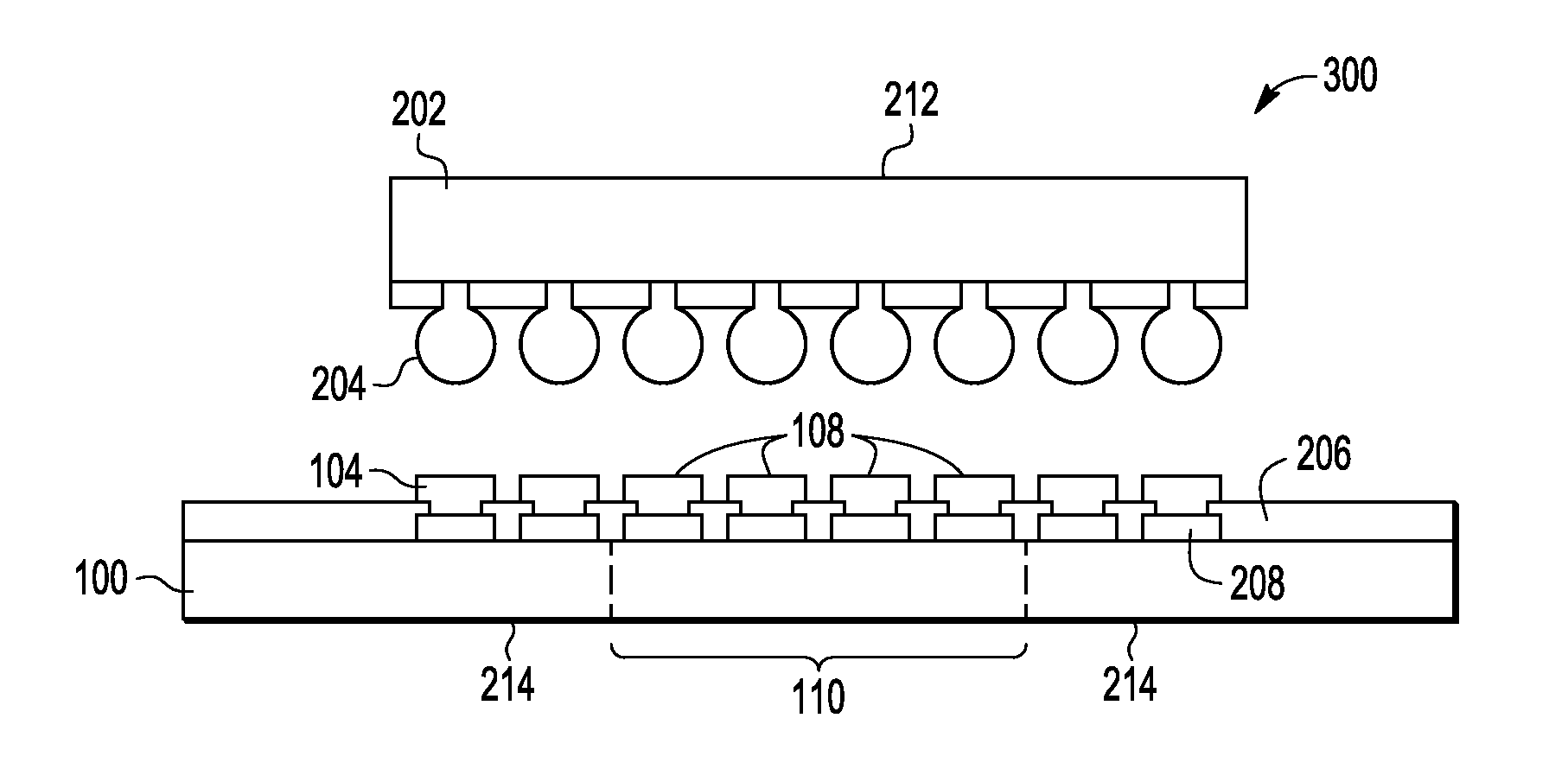
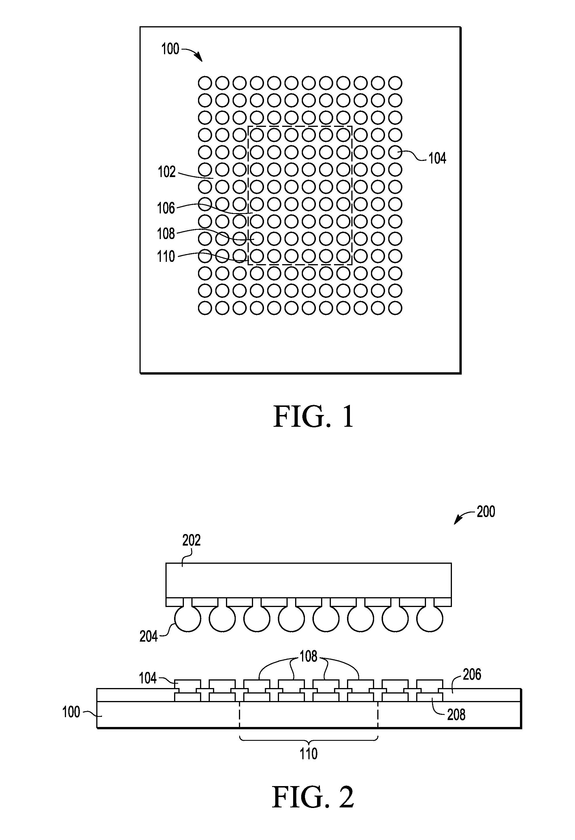
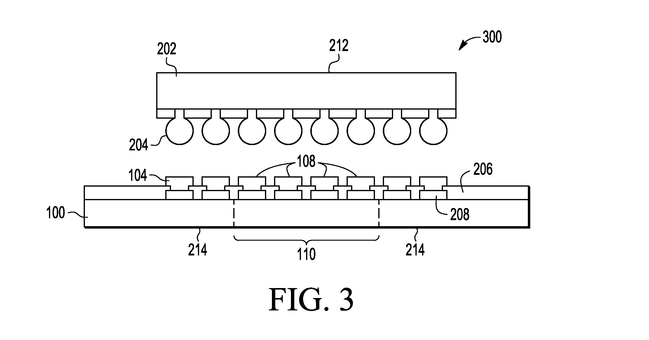
[0009]Embodiments of methods and semiconductor devices disclosed herein substantially reduce or even eliminate white bumps or interlayer dielectric (ILD) delamination in a semiconductor die in a flip chip package. The white bumps form generally at the outer edges of the semiconductor die and are caused by stress that occurs during cool down after a reflow process to attach a flip chip die to a package substrate. To eliminate the white bumps, electrically conductive die attach material referred to as solder cladding on package substrate with a relatively higher solidus temperature can be used for an inner section of the package substrate contacts compared to the solidus temperature of die attach material or cladding used for the contacts in the outer sections of the package substrate. As the assembled device cools down, the die attach material on the inner section solidifies before the die attach material on the outer sections of the die / package substrate, thus reducing the stress tr...
PUM
| Property | Measurement | Unit |
|---|---|---|
| solidus temperature | aaaaa | aaaaa |
| solidus temperature | aaaaa | aaaaa |
| solidus temperature | aaaaa | aaaaa |
Abstract
Description
Claims
Application Information