Microbolometer array with improved performance

a microbolometer and array technology, applied in the direction of instruments, radiation controlled devices, optical radiation measurement, etc., can solve the problems of increasing the sensitivity of the microbolometer without increasing the response time, and also limited the mass of the thermometric elemen

Active Publication Date: 2014-08-14
CENT NAT DE LA RECHERCHE SCI +2
View PDF5 Cites 44 Cited by
  • Summary
  • Abstract
  • Description
  • Claims
  • Application Information

AI Technical Summary

Benefits of technology

[0034]For example, for a given microbolometer pixel, said structures are identical and distributed over the area of the microbolometer pixel. For example, the MIM structures have a square shape optimized to absorb at a given wavelength of the desired absorption spectrum, allowing a larger microbolometer pixel to be produced, the effective absorption area of all the MIM structures allowing all or almost all of the area of the microbolometer pixel to be covered.
[0035]Alternatively, for a given microbolometer pixel, at least two of said MIM structures are different and able to generate, under said incident radiation, a plasmon resonance at at least two separate wavelengths in said spectral band, thus allowing the spectral response of the microbolometer pixel to be “shaped”.
[0036]According to another variant embodiment, the absorber element of at least one of the microbolometer pixels comprises at least one second MIM structure superposed on said first MIM structure, said first and second structures being able to have a resonant absorption of the incident radiation at at least two separate wavelengths in said spectral band, and sharing a common metallic film. This configuration allows the spectral response of the microbolometer pixel to be shaped, even in the case of small pixels, the structures being stacked, for example in the centre of the pixel.

Problems solved by technology

As a result the sensitivity of the microbolometer is increased without increasing the response time, the mass of the thermometric element also being limited.

Method used


Image

  • Microbolometer array with improved performance
  • Microbolometer array with improved performance
  • Microbolometer array with improved performance

Examples


Embodiment Construction

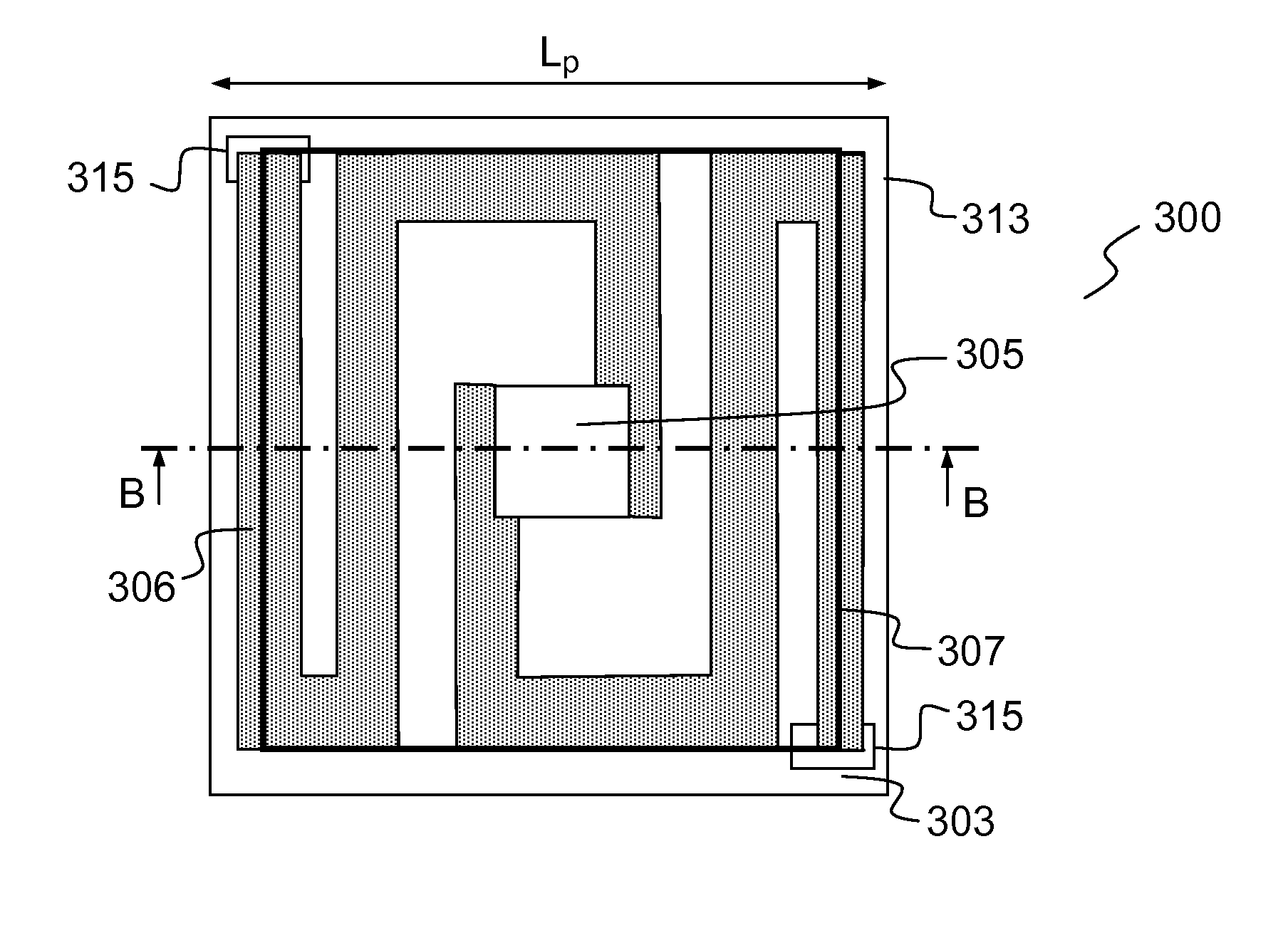
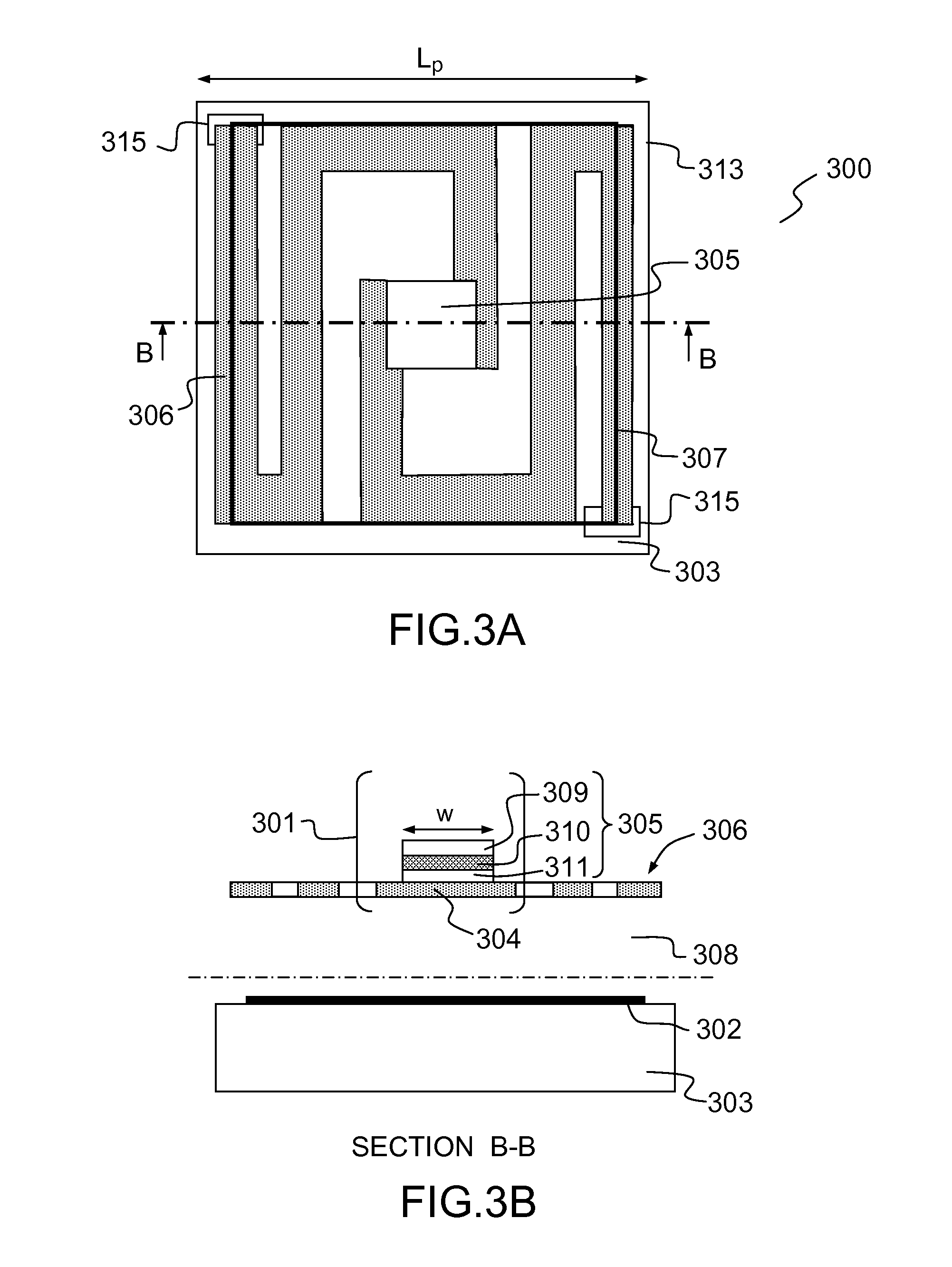
[0065]FIGS. 3A and 3B respectively illustrate a top view and a cross-sectional view of a first exemplary microbolometer pixel according to the invention for detecting radiation having a wavelength in a given spectral band, for example in the infrared. The elements shown in the figures of the present description are not shown to scale, so as to make the drawings more legible. The microbolometer pixel 300 comprises a membrane (301, FIG. 3B) that is suspended over a supporting substrate 303 by supporting elements. The membrane 301 is formed by an element 305 for absorbing incident radiation and a thermometric element 302 making thermal contact with the absorber preferably over its whole surface or nearly its whole surface in order to warm up homogeneously, but electrically insulated from it, for example by means of an insulating film, for example made of silicon nitride. The microbolometer pixel 300 advantageously comprises arms 306 for thermally insulating the thermometric element, on...


PUM


Abstract

According to one aspect, the invention relates to a microbolometer array for thermal detection of light radiation in a given spectral band, comprising a supporting substrate and an array of microbolometers (300) of given dimensions, arranged in an array. Each of said microbolometers comprises a membrane (301) suspended above said supporting substrate, said membrane consisting of an element (305) for absorbing the incident radiation and a thermometric element (304) in thermal contact with the absorber, electrically insulated from said absorber element. The absorber element comprises at least one first metal/insulator/metal (MIM) structure comprising a multilayer of three superposed films of submicron-order thickness i.e. a first metallic film (311), a dielectric film (310), and a second metallic film (309), said MIM structure being able to have a resonant absorption of said incident radiation at at least one wavelength in said spectral band. The area of the microbolometer pixel covered by said membrane (301) is less than or equal to half of the total area of the microbolometer pixel.

Description

TECHNICAL FIELD OF THE INVENTION[0001]The present invention relates to a microbolometer array with improved performance, especially for detecting radiation in the infrared.PRIOR ART[0002]Uncooled infrared detectors have for several decades been the subject of intense research and development. Among such detectors, the market for resistive microbolometers is, at the present time, experiencing substantial growth, especially for civil applications (home electronics, driver or pilot assistance, night vision, fire investigation, etc.). Resistive microbolometers are particularly suited to detection in the infrared, and more particularly to detection in band III (8-12 μm), corresponding to one of the spectral bands that is transmitted through the atmosphere allowing heat emitted by objects at room temperature or by living creatures to be observed.[0003]A microbolometer array, intended to be used in a camera, may be fabricated in the form of an array of detecting elements, called in the res...

Claims


Application Information

Patent Timeline
Patent Type & Authority Applications(United States)
IPC IPC(8): G01J5/20H04N5/33H01L27/146
CPCG01J5/20G01J2005/204H04N5/33H01L27/14685G01J5/08G01J5/0853
Inventor KOECHLIN, CHARLIEBOUCHON, PATRICKHAIDAR, RIADPELOUARD, JEAN-LUCYON, JEAN-JACQUESDESCHAMPS, JOELPARDO, FABRICECOLLIN, STEPHANE
Owner CENT NAT DE LA RECHERCHE SCI
Why Eureka
Try Eureka