Semiconductor device including electromagnetic absorption and shielding

a technology of electromagnetic absorption and shielding, which is applied in the direction of cross-talk/noise/interference reduction, printed circuit aspects, printed circuit manufacturing, etc., can solve the problems of unwanted signals (interference or noise), unwanted interference or noise, and electric shortening

Active Publication Date: 2014-08-21
SANDISK INFORMATION TECH SHANGHAI
View PDF7 Cites 34 Cited by
  • Summary
  • Abstract
  • Description
  • Claims
  • Application Information

AI Technical Summary

Benefits of technology

[0068]In another embodiment, the present technology relates to a semiconductor device, comprising: a substrate; a solder mask layer on the substrate, the solder mask layer including a first absorbing material for absorbing at least one of EMI and RFI; one or more semiconductor die affixed and electrically connected to the substrate; a molding compound encapsulating at least the one or more semiconductor die; and a layer provided on the molding compound, the layer including a second absorbing material for absorbing at least one of EMI and RFI.
[0069]In a further embodiment, the present technology relates to a semiconductor device, comprising: a substrate; a solder mask layer on the substrate, the solder mask layer including a first absorbing material for absorbing at least one of EMI and RFI; one or more semiconductor die affixed and electrically connected to the substrate; a molding compound encapsulating at least the one or more semiconductor die; and first and second layers provided on the molding compound, the first layer including a second absorbing material for absorbing at least one of EMI and RFI, and the second layer including a conductive material for shielding the semiconductor device against at least one of EMI and RFI.
[0070]In a still further embodiment, the present technology relates to a method of shielding a semiconductor device from at least one of EMI and RFI, comprising the steps of: (a) mounting one or more semiconductor die on a substrate; (b) encapsulating the one or more semiconductor die on the substrate in molding compound; and (c) completely encapsulating the one or more semiconductor die in one or more layers of absorbing material that absorb at least one of EMI and RFI.

Problems solved by technology

In addition to the height of the bond wires 30 themselves, additional space must be left above the bond wires, as contact of the bond wires 30 of one die with the next die above may result in an electrical short.
EMI is the induction of electromagnetic radiation, which is emitted by electrical circuits carrying rapidly changing signals, as a by-product of their normal operation to other circuits, which causes unwanted signals (interference or noise).
RFI is transmission of radiofrequency electromagnetic radiation from one circuit to another, also causing unwanted interference or noise.
While preventing interference, these conventional solutions have other disadvantages which make inclusion of such features at the package level undesirable.
However, conventional absorptive solutions have not satisfactorily addressed EMI and / or RFI in a semiconductor package.

Method used


Image

  • Semiconductor device including electromagnetic absorption and shielding
  • Semiconductor device including electromagnetic absorption and shielding
  • Semiconductor device including electromagnetic absorption and shielding

Examples


Embodiment Construction

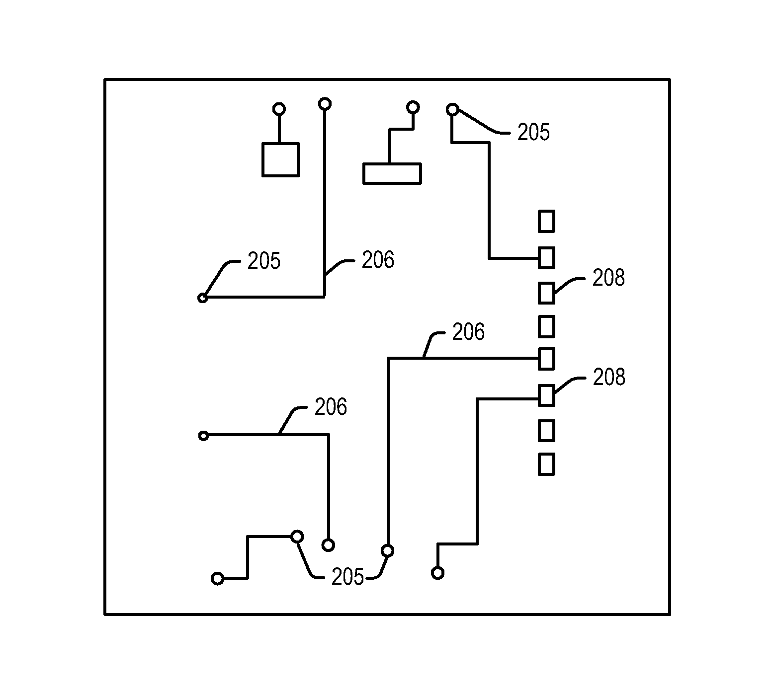
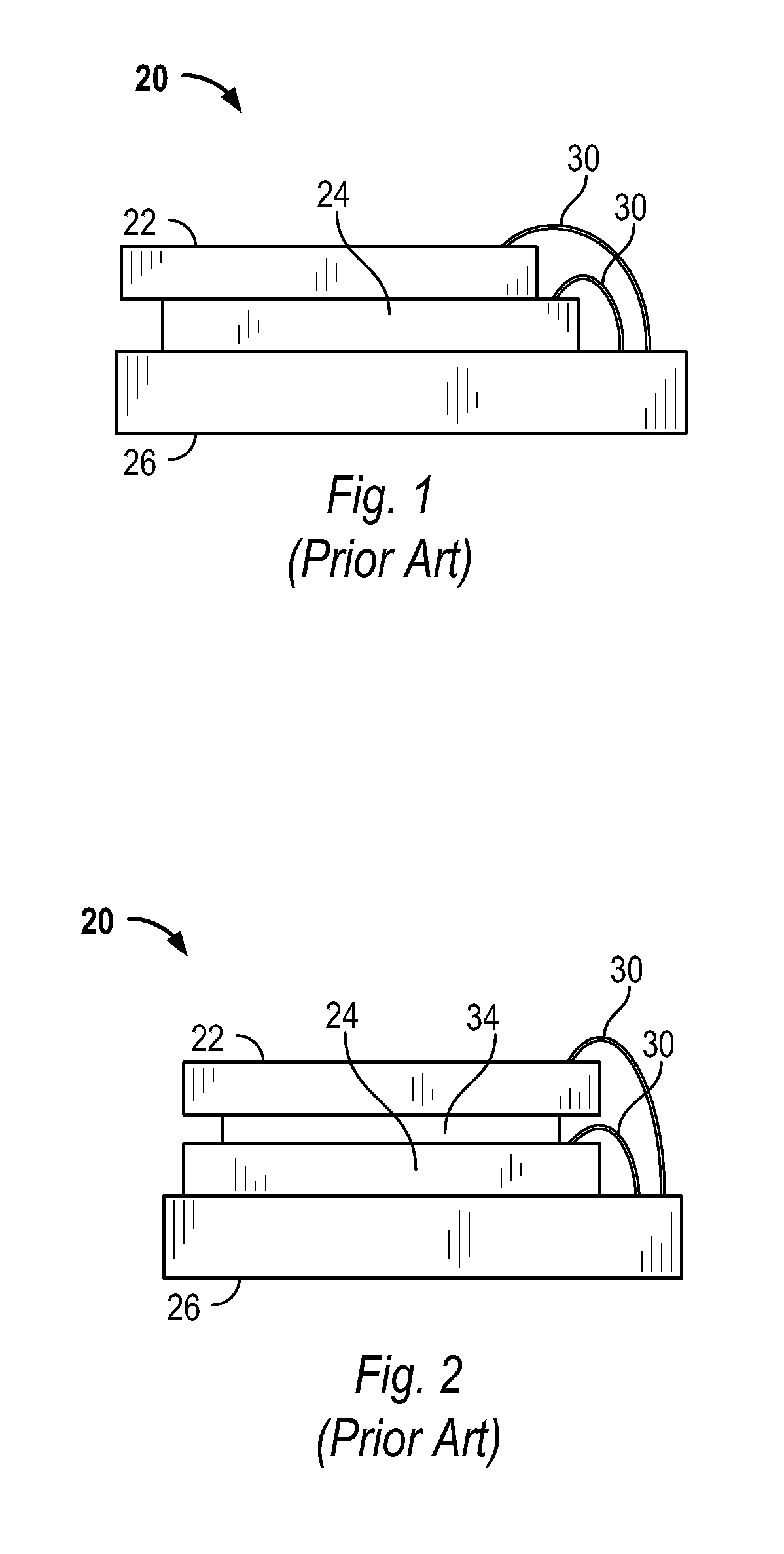
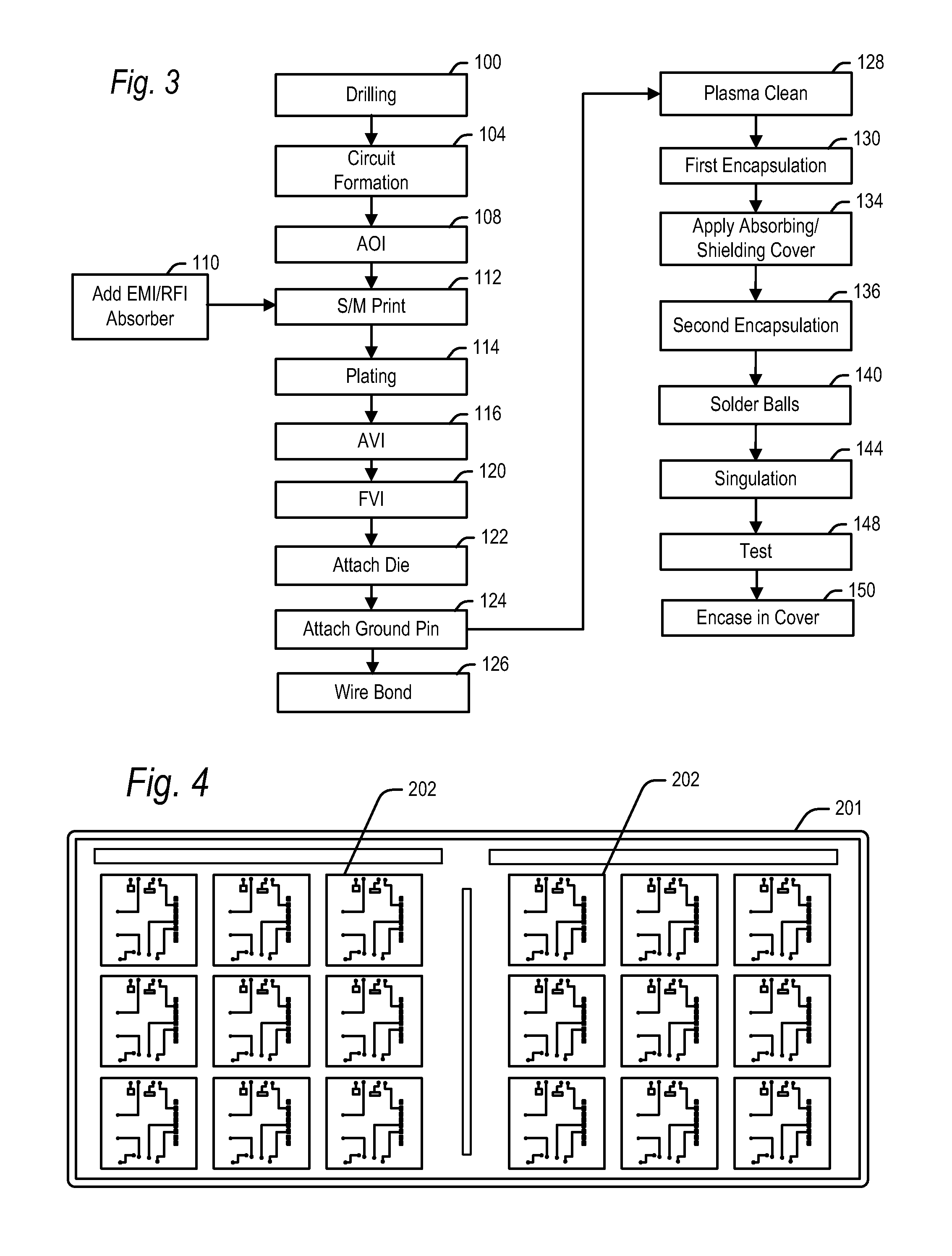
[0026]Embodiments will now be described with reference to FIGS. 3 through 18, which relate to a semiconductor package including EMI and RFI shielding and absorption. It is understood that the present invention may be embodied in many different forms and should not be construed as being limited to the embodiments set forth herein. Rather, these embodiments are provided so that this disclosure will be thorough and complete and will fully convey the invention to those skilled in the art. Indeed, the invention is intended to cover alternatives, modifications and equivalents of these embodiments, which are included within the scope and spirit of the invention as defined by the appended claims. Furthermore, in the following detailed description of the present invention, numerous specific details are set forth in order to provide a thorough understanding of the present invention. However, it will be clear to those of ordinary skill in the art that the present invention may be practiced wit...


PUM


Abstract

A semiconductor device is disclosed including material for absorbing EMI and/or RFI The device includes a substrate (202), one or more semiconductor die (224,225), and molding compound around the one or more semiconductor die (224,225). The material for absorbing EMI and/or RFI may be provided within or on a solder mask layer (210) on the substrate (202). The device may further include EMI/RFI-absorbing material around the molding compound and in contact with the EMI/RFI-absorbing material on the substrate to completely enclose the one or more semiconductor die in EMI/RFI-absorbing material.

Description

BACKGROUND OF THE INVENTION[0001]1. Field[0002]Embodiments of the present invention relate to semiconductor devices.[0003]2. Description of Related Art[0004]The strong growth in demand for portable consumer electronics is driving the need for high-capacity storage devices. Non-volatile semiconductor memory devices, such as flash memory storage cards, are becoming widely used to meet the ever-growing demands on digital information storage and exchange. Their portability, versatility and rugged design, along with their high reliability and large capacity, have made such memory devices ideal for use in a wide variety of electronic devices, including for example digital cameras, digital music players, video game consoles, PDAs and cellular telephones.[0005]While a wide variety of packaging configurations are known, flash memory storage cards may in general be fabricated as system-in-a-package (SiP) or multichip modules (MCM), where a plurality of die are mounted on a substrate in a stac...

Claims


Application Information

Patent Timeline
Patent Type & Authority Applications(United States)
IPC IPC(8): H01L23/552H01L21/56
CPCH01L2224/04042H01L2225/0651H01L2924/00H01L2924/19041H01L2224/48147H01L21/56H01L2924/1434H01L2224/48227H05K3/3452H01L23/49811H01L2924/15313H01L2924/19043H05K1/0218H01L23/295H01L25/18H01L2924/1438H01L23/552H01L2224/06155H01L2225/06562H01L2224/97H01L24/48H01L2224/48145H01L25/0657H01L2924/19105H01L2224/49113H05K1/0298H05K2201/0215H01L2224/85H05K2201/083H01L2924/19042H01L2924/3025H01L23/3135H01L2225/06537H01L2225/06506H01L23/49894H01L2924/1433H01L24/97H01L24/06H01L2924/15311H01L2224/05554H01L2924/181H01L2924/12042H01L2924/00014H01L24/49H01L2924/00012H01L2224/45099H01L2224/45015H01L2924/207
Inventor HUANG, DACHENGBAI, YEQIAN, KAIYOUCHIU, CHIN-TIEN
Owner SANDISK INFORMATION TECH SHANGHAI
Why Eureka
Try Eureka